.png)

Introduction#
I was recently in the market for a new FPGA to start building my upcoming projects on.
Due to the scale of my upcoming projects a Xilinx series 7 UltraScale+ FPGA of the Virtex family would be perfect, but a Kintex series FPGA will be sufficient for early prototyping. Due to not wanting to part ways with the eye watering amounts of money that is required for an Vivado enterprise edition license my choice was effectively narrowed to the FPGA chips available under the WebPack version of Vivado.
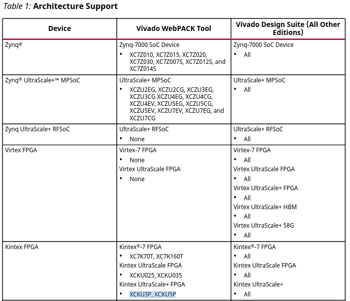 Xilinx supported boards per Vivado edition
Unsurprisingly Xilinx are well aware of how top of the range the Virtex series are, and doesn’t offer any Virtex UltraScale+ chips with the webpack license. That said, they do offer support for two very respectable Kintex UltraScale+ FPGA models, the XCKU3P and the XCKU5P.
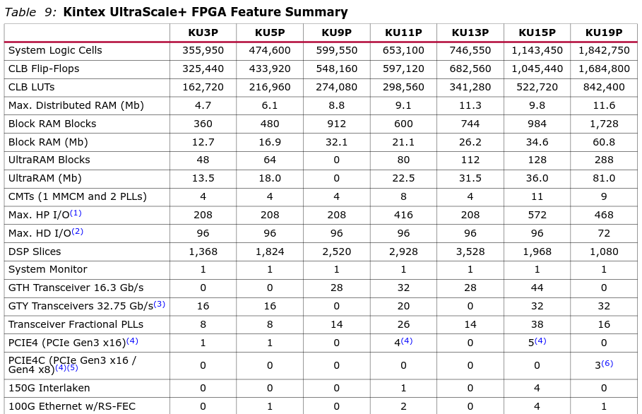 Xiling product guide, overview for the Kintex UltraScale+ series
These two chips are far from being small hobbyist toys, with the smaller XCUK3P already boasting +162K LUTs and 16 GTY transceivers, capable, depending on the physical constraints imposed by the chip packaging of operating at up to 32.75Gb/s.
Now that the chip selection has been narrowed down I set out to look for a dev board.
My requirements for the board where that it featured :
- at least 2 SFP+ or 1 QSFP connector
- a JTAG interface
- a PCIe interface at least x8 wide
As to where to get the board from, my options where :
- Design the board myself
- Get the AXKU5 or AXKU3 from Alinx
- See what I could unearth on the second hand market
Although option 1 could have been very interesting, designing a dev board with both a high speed PCIe and ethernet interface was not the goal of today’s project.
As for option 2, Alinx is newer vendor that is still building up its credibility in the west, their technical documentation is a bit sparse, but the feedback seems to be positive with no major issues being reported. Most importantly, Alinx provided very fairly priced development boards in the 900 to 1050 dollar range ( +150$ for the HPC FMC SFP+ extension board ). Although these are not cheap by any metric, compared to the competitions price point, they are the best value.
Option 2 was coming up ahead until I stumbled upon this ebay listing :
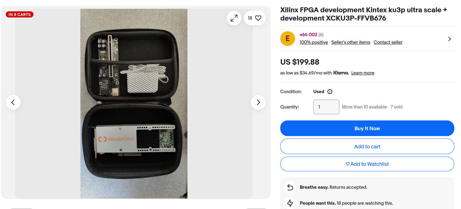 Ebay listing for a decommissioned Alibaba Cloud accelerator FPGA
But I like a challenge, and the appeal of unlocking the 200$ Kintex UltraScale+ development board was too great to ignore.
As such, I aim for this article to become the documentation paving the way to though this mirage.
The debugger challenge#
Xilinx’s UG908 Programming and Debugging User Guide (Appendix D) specifies their blessed JTAG probe ecosystem for FPGA configuration and debug. Rather than dropping $100+ on yet another proprietary dongle that’ll collect dust after the project ends, I’m exploring alternatives. The obvious tradeoff: abandoning Xilinx’s toolchain means losing ILA integration. However, the ILA fundamentally just captures samples and streams them via JTAG USER registers, there’s nothing preventing us from building our own logic analyzer with equivalent functionality and a custom host interface.
Enter OpenOCD. While primarily targeting ARM/RISC-V SoCs, it maintains an impressive database of supported probe hardware and provides granular control over JTAG operations. More importantly, it natively supports SVF (Serial Vector Format), a vendor-neutral bitstream format that Vivado can export.
The documentation landscape is admittedly sparse for anything beyond 7-series FPGAs, and the most recent OpenOCD documentation I could unearth was focused on Zynq ARM core debugging rather than fabric configuration. But the fundamentals remain sound: JTAG is JTAG, SVF is standardized, and the boundary scan architecture hasn’t fundamentally changed.
The approach should be straightforward: generate SVF from Vivado, feed it through OpenOCD with a commodity JTAG adapter, and validate the configuration. Worst case, we’ll need to patch some adapter-specific quirks or boundary scan chain register addresses. Time to find out if this theory holds up in practice.
The plan#
So, to resume, the current plan is to buy a second hand hardware accelerator of eBay at a too good to be true price, and try to configure it
with an unofficial probe using open source software without any clear official support.
The answer to the obvious question you are thinking if you, like me, have been around the block a few times is: many things.
As such, we need a plan for approaching this. The goal of this plan is to outline incremental steps that will build upon themselves with the end goal of being able to use this as a dev board.
1 - Confirming the board works#
First order of business will be to confirm the board is showing signs of working as intended.
There is a high probability that the flash wasn’t wiped before this board was sold off, as such the previous bitstream should still be in the flash. Given this board was used as an accelerator, we should be able to use that to confirm the board is working by either checking if the board is presenting itself as a PCIe endpoint or if the SFP’s are sending the ethernet PHY idle sequence.
2 - Connecting a debugger to it#
The next step is going to be to try and connect the debugger. The eBay listing advertised there is a JTAG interface, but the picture is grainy enough that where that JTAG is and what pins are available is unclear.
Additionally, we have no indication of what devices are daisy chained together onto the JTAG scan chain. This is an essential question for flashing over JTAG, so it will need to be figured out.
At this point, it would also be strategic to try and do some more probing into the FPGA via JTAG. Xilinx FPGAs exposes a handful of useful system registers accessible over JTAG. The most well known of these interfaces is the SYSMON, which allows us, among other things, to get real time temperature and voltage reading from inside the chip. Although openOCD doesn’t have SYSMON support out of the box it would be worth while to build it, to :
- Familiarise myself with openOCD scripting, this might come in handy when building my ILA replacement down the line
- Having an easy side channel to monitor FPGA operating parameters
- Make a contribution to openOCD as it have support for the interfacing with XADC but not SYSMON
3 - Figuring out the Pinout#
The hardest part will be figuring out the FPGA’s pinout and my clock sources. The questions that need answering are :
- what external clocks sources do I have, what are there frequencies and which pins are they connected to
- which transceivers are the SFPs connected to
- which transceivers is the PCIe connected to
4 - Writing a bitstream#
For now I will be focusing on writing a temporary configurations over JTAG to the CCLs and not re-writing the flash.
That plan is to trying writing either the bitstream directly though openOCD’s virtex2 + pld drivers, or by replaying the SVF generated by Vivado.
Since I believe a low iteration time is paramount to project velocity and getting big things done, I also want automatize all of the Vivado flow from taking the rtl to the SVF generation.
Simple enough ?
Liveness test#
A few days later my prize arrived via express mail.
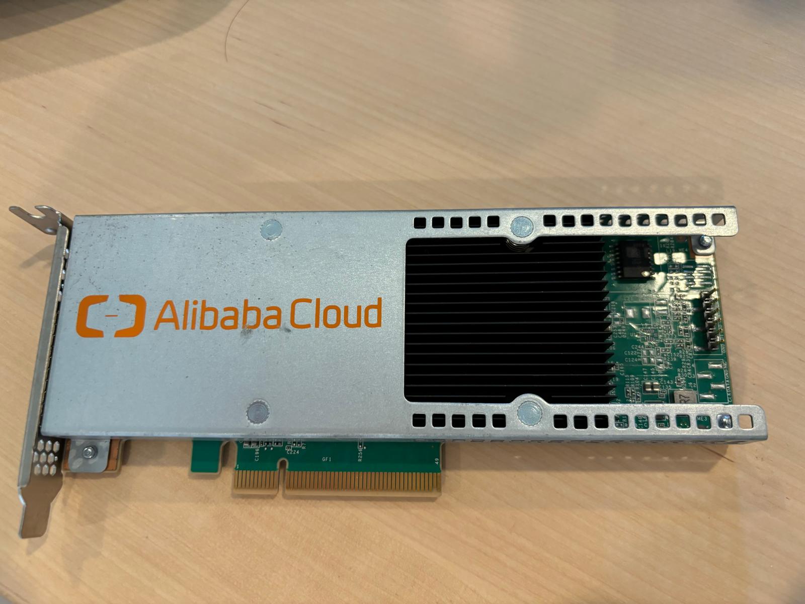 My prized Kintex UltraScale+ FPGA board also known as the decommissioned Alibaba cloud accelerator. Jammed transceiver now safely removed.
Unexpectedly it even came with a free 25G SFP28 Huawei transceiver rated for a 300m distance and a single 1m long OS2 fiber patch cable. This was likely not intentional as the transceiver was jammed in the SFP cage, but it was still very generous of them to include the fiber patch cable.
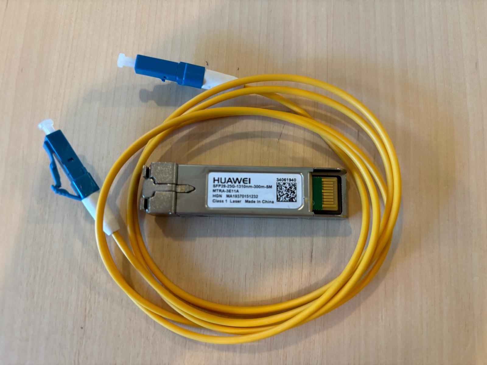 Free additional SFP28-25G-1310nm-300m-SM Huawei transceiver, and 1m long OS2 patch cable
The board also came with a travel case and half of a PCIe to USB adapter and a 12V power supply that one could use to power the board as a standalone device. Although this standalone configuration will not be of any use to me, for those looking to develop just networking interfaces without any PCIe interface, this could come in handy.
Overall the board looked a little worn, but both the transceiver cages and PCIe connectors didn’t look to be damaged.
Standalone configuration#
Before real testing could start I first did a small power-up test using the PCIe to USB adapter that the seller provided. I was able to do a quick check using the LEDs and the FPGAs dissipated heat that the board seemed to be powering up at a surface level (pun intended).
PCIe interface#
As a reminder, this next section relies on the flash not having been wiped and still containing the previous user’s design.
Since I didn’t want to directly plug mystery hardware into my prized build server, I decided to use a Raspberry Pi 5 as my sacrificial test device and got myself an external PCIe adapter.
It just so happened that the latest Raspberry Pi version, the Pi 5, now features an external PCIe Gen 2.0 x1 interface. Though our FPGA can handle up to a PCIe Gen 3.0 and the board had a x8 wide interface, since PCIe standard is backwards compatible and the number of lanes on the interface can be downgraded, plugging our FPGA with this Raspberry Pi will work.
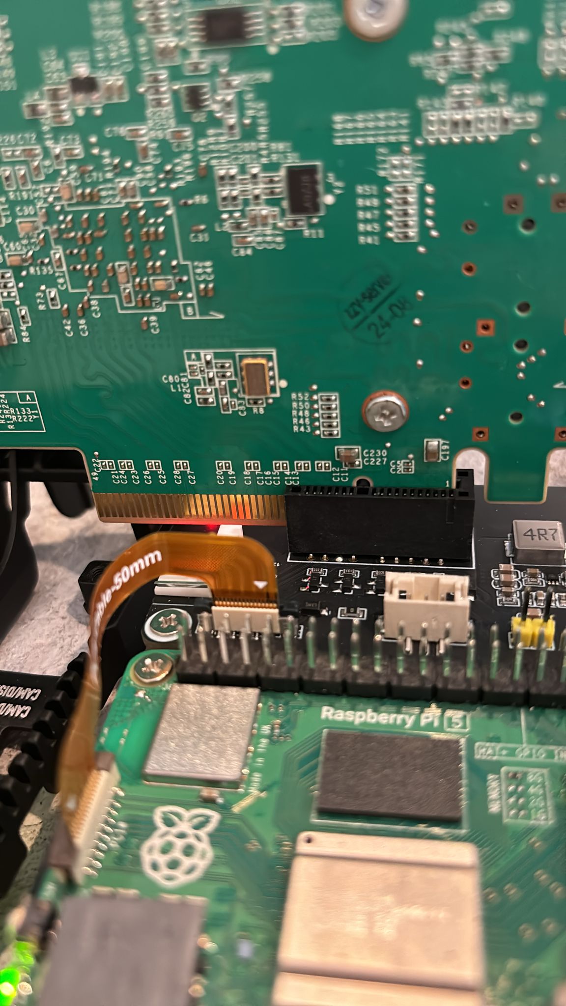
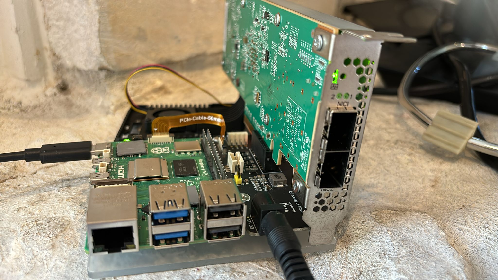 FPGA board connected to the Raspberry Pi 5 via the PCIe to PCIe x1 adapter
After both the Raspberry and the FPGA were booted, I SSHed into my rpi and started looking for the PCIe enumeration sequence logged from the Linux PCIe core subsystem.
dmesg log :
[ 0.388790] pci 0000:00:00.0: [14e4:2712] type 01 class 0x060400 [ 0.388817] pci 0000:00:00.0: PME# supported from D0 D3hot [ 0.389752] pci 0000:00:00.0: bridge configuration invalid ([bus 00-00]), reconfiguring [ 0.495733] brcm-pcie 1000110000.pcie: link up, 5.0 GT/s PCIe x1 (!SSC) [ 0.495759] pci 0000:01:00.0: [dabc:1017] type 00 class 0x020000Background information#
Since most people might not be intimately as familiar with PCIe terminology, allow me to quickly document what is going on here.
0000:00:00.0: is the identifier of a specific PCIe device connected through the PCIe network to the kernel, it read as domain:bus:device.function.
[14e4:2712]: is the device’s [vendor id:device id], these vendor id identifiers are assigned by the PCI standard body to hardware vendors. Vendors are then free to define there own vendor id’s.
The full list of official vendor id’s and released device id can be found : https://admin.pci-ids.ucw.cz/read/PC/14e4 or in the linux kernel code : https://github.com/torvalds/linux/blob/7aac71907bdea16e2754a782b9d9155449a9d49d/include/linux/pci_ids.h#L160-L3256
type 01: PCIe has two types of devices, bridges allowing the connection of multiple downstream devices to an upstream device, and endpoints are the leafs. Bridges are of type 01 and endpoints of type 00.
class 0x60400: is the PCIe device class, it categorizes the kind of function the device performs. It uses the following format 0x[Base Class (8 bits)][Sub Class (8 bits)][Programming Interface (8 bits)], ( note : the sub class field might be unused ).
A list of class and sub class identifiers can be found: https://admin.pci-ids.ucw.cz/read/PD or again in the linux codebase : https://github.com/torvalds/linux/blob/7aac71907bdea16e2754a782b9d9155449a9d49d/include/linux/pci_ids.h#L15-L158
Dmesg log#
The two most interesting lines of the dmesg log are :
[ 0.388790] pci 0000:00:00.0: [14e4:2712] type 01 class 0x060400 [ 0.495759] pci 0000:01:00.0: [dabc:1017] type 00 class 0x020000Firstly the PCIe subsystem logs that at 0000:00:00.0 it has discovered a Broadcom BCM2712 PCIe Bridge ( vendor id 14e4, device id 0x2712 ).This bridge (type 01) class 0x0604xx tells us it is a PCI-to-PCI bridge, meaning it is essentially creating additional PCIe lanes downstream for endpoint devices or additional bridges.
The subsystem then discovers a second device at 0000:01:00.0, this is an endpoint (type 00), and class 0x02000 tells us it is an ethernet networking equipment.
Of note dabc doesn’t correspond to a known vendor id.
When designing a PCIe interface in hardware these
are parameters we can configured. Additionally, among the different ways Linux uses to identify which driver to load for a PCIe device
the vendor id and device id can be used for matching. Supposing we are implementing custom logic, in order to prevent any bug where the wrong driver
might be loaded, it is best to use a separate vendor id.
This also helps identify your custom accelerator at a glance and use it to load your custom driver.
As such, it is not surprising to see an unknown vendor id appear for an FPGA, this with the class as an ethernet networking device is a strong hint this is our board.
Full PCIe device status#
Dmesg logs have already given us a good indication that our FPGA board and its PCIe interface was working but to confirm with certainty that the device with vendor id dabc is our FPGA we now turn to lspci. lspci -vvv is the most verbose output and gives us a full overview of the detected PCIe devices capabilities and current configurations.
Broadcom bridge:
0000:00:00.0 PCI bridge: Broadcom Inc. and subsidiaries BCM2712 PCIe Bridge (rev 21) (prog-if 00 [Normal decode]) Control: I/O- Mem+ BusMaster+ SpecCycle- MemWINV- VGASnoop- ParErr- Stepping- SERR- FastB2B- DisINTx- Status: Cap+ 66MHz- UDF- FastB2B- ParErr- DEVSEL=fast >TAbort- <TAbort- <MAbort- >SERR- <PERR- INTx- Latency: 0 Interrupt: pin A routed to IRQ 38 Bus: primary=00, secondary=01, subordinate=01, sec-latency=0 Memory behind bridge: [disabled] [32-bit] Prefetchable memory behind bridge: 1800000000-182fffffff [size=768M] [32-bit] Secondary status: 66MHz- FastB2B- ParErr- DEVSEL=fast >TAbort- <TAbort- <MAbort- <SERR- <PERR- BridgeCtl: Parity- SERR- NoISA- VGA- VGA16- MAbort- >Reset- FastB2B- PriDiscTmr- SecDiscTmr- DiscTmrStat- DiscTmrSERREn- Capabilities: [48] Power Management version 3 Flags: PMEClk- DSI- D1- D2- AuxCurrent=0mA PME(D0+,D1-,D2-,D3hot+,D3cold-) Status: D0 NoSoftRst+ PME-Enable- DSel=0 DScale=1 PME- Capabilities: [ac] Express (v2) Root Port (Slot-), MSI 00 DevCap: MaxPayload 512 bytes, PhantFunc 0 ExtTag- RBE+ DevCtl: CorrErr- NonFatalErr- FatalErr- UnsupReq- RlxdOrd+ ExtTag- PhantFunc- AuxPwr+ NoSnoop+ MaxPayload 512 bytes, MaxReadReq 512 bytes DevSta: CorrErr- NonFatalErr- FatalErr- UnsupReq- AuxPwr- TransPend- LnkCap: Port #0, Speed 5GT/s, Width x1, ASPM L0s L1, Exit Latency L0s <2us, L1 <4us ClockPM+ Surprise- LLActRep- BwNot+ ASPMOptComp+ LnkCtl: ASPM Disabled; RCB 64 bytes, Disabled- CommClk- ExtSynch- ClockPM- AutWidDis- BWInt- AutBWInt- LnkSta: Speed 5GT/s, Width x1 TrErr- Train- SlotClk+ DLActive- BWMgmt- ABWMgmt+ RootCap: CRSVisible+ RootCtl: ErrCorrectable- ErrNon-Fatal- ErrFatal- PMEIntEna+ CRSVisible+ RootSta: PME ReqID 0000, PMEStatus- PMEPending- DevCap2: Completion Timeout: Range ABCD, TimeoutDis+ NROPrPrP- LTR+ 10BitTagComp- 10BitTagReq- OBFF Via WAKE#, ExtFmt- EETLPPrefix- EmergencyPowerReduction Not Supported, EmergencyPowerReductionInit- FRS- LN System CLS Not Supported, TPHComp- ExtTPHComp- ARIFwd+ AtomicOpsCap: Routing- 32bit- 64bit- 128bitCAS- DevCtl2: Completion Timeout: 50us to 50ms, TimeoutDis- LTR- 10BitTagReq- OBFF Disabled, ARIFwd- AtomicOpsCtl: ReqEn- EgressBlck- LnkCap2: Supported Link Speeds: 2.5-5GT/s, Crosslink- Retimer- 2Retimers- DRS+ LnkCtl2: Target Link Speed: 5GT/s, EnterCompliance- SpeedDis- Transmit Margin: Normal Operating Range, EnterModifiedCompliance- ComplianceSOS- Compliance Preset/De-emphasis: -6dB de-emphasis, 0dB preshoot LnkSta2: Current De-emphasis Level: -6dB, EqualizationComplete- EqualizationPhase1- EqualizationPhase2- EqualizationPhase3- LinkEqualizationRequest- Retimer- 2Retimers- CrosslinkRes: unsupported, DRS- DownstreamComp: Link Up - Present Capabilities: [100 v1] Advanced Error Reporting UESta: DLP- SDES- TLP- FCP- CmpltTO- CmpltAbrt- UnxCmplt- RxOF- MalfTLP- ECRC- UnsupReq- ACSViol- UEMsk: DLP- SDES- TLP- FCP- CmpltTO- CmpltAbrt- UnxCmplt- RxOF- MalfTLP- ECRC- UnsupReq- ACSViol- UESvrt: DLP+ SDES+ TLP- FCP+ CmpltTO- CmpltAbrt- UnxCmplt- RxOF+ MalfTLP+ ECRC- UnsupReq- ACSViol- CESta: RxErr- BadTLP- BadDLLP- Rollover- Timeout- AdvNonFatalErr- CEMsk: RxErr- BadTLP- BadDLLP- Rollover- Timeout- AdvNonFatalErr+ AERCap: First Error Pointer: 00, ECRCGenCap+ ECRCGenEn- ECRCChkCap+ ECRCChkEn- MultHdrRecCap- MultHdrRecEn- TLPPfxPres- HdrLogCap- HeaderLog: 00000000 00000000 00000000 00000000 RootCmd: CERptEn+ NFERptEn+ FERptEn+ RootSta: CERcvd- MultCERcvd- UERcvd- MultUERcvd- FirstFatal- NonFatalMsg- FatalMsg- IntMsg 0 ErrorSrc: ERR_COR: 0000 ERR_FATAL/NONFATAL: 0000 Capabilities: [160 v1] Virtual Channel Caps: LPEVC=0 RefClk=100ns PATEntryBits=1 Arb: Fixed- WRR32- WRR64- WRR128- Ctrl: ArbSelect=Fixed Status: InProgress- VC0: Caps: PATOffset=00 MaxTimeSlots=1 RejSnoopTrans- Arb: Fixed- WRR32- WRR64- WRR128- TWRR128- WRR256- Ctrl: Enable+ ID=0 ArbSelect=Fixed TC/VC=ff Status: NegoPending- InProgress- Capabilities: [180 v1] Vendor Specific Information: ID=0000 Rev=0 Len=028 <?> Capabilities: [240 v1] L1 PM Substates L1SubCap: PCI-PM_L1.2+ PCI-PM_L1.1+ ASPM_L1.2+ ASPM_L1.1+ L1_PM_Substates+ PortCommonModeRestoreTime=8us PortTPowerOnTime=10us L1SubCtl1: PCI-PM_L1.2- PCI-PM_L1.1- ASPM_L1.2- ASPM_L1.1- T_CommonMode=1us LTR1.2_Threshold=0ns L1SubCtl2: T_PwrOn=10us Capabilities: [300 v1] Secondary PCI Express LnkCtl3: LnkEquIntrruptEn- PerformEqu- LaneErrStat: 0 Kernel driver in use: pcieportFPGA board:
0000:01:00.0 Ethernet controller: Device dabc:1017 Subsystem: Red Hat, Inc. Device a001 Control: I/O- Mem- BusMaster- SpecCycle- MemWINV- VGASnoop- ParErr- Stepping- SERR- FastB2B- DisINTx- Status: Cap+ 66MHz- UDF- FastB2B- ParErr- DEVSEL=fast >TAbort- <TAbort- <MAbort- >SERR- <PERR- INTx- Region 0: Memory at 1820000000 (64-bit, prefetchable) [disabled] [size=2K] Region 2: Memory at 1800000000 (64-bit, prefetchable) [disabled] [size=512M] Capabilities: [40] Power Management version 3 Flags: PMEClk- DSI- D1- D2- AuxCurrent=0mA PME(D0-,D1-,D2-,D3hot-,D3cold-) Status: D0 NoSoftRst+ PME-Enable- DSel=0 DScale=0 PME- Capabilities: [70] Express (v2) Endpoint, MSI 00 DevCap: MaxPayload 1024 bytes, PhantFunc 0, Latency L0s <64ns, L1 <1us ExtTag+ AttnBtn- AttnInd- PwrInd- RBE+ FLReset- SlotPowerLimit 0W DevCtl: CorrErr+ NonFatalErr+ FatalErr+ UnsupReq+ RlxdOrd+ ExtTag+ PhantFunc- AuxPwr- NoSnoop+ MaxPayload 512 bytes, MaxReadReq 512 bytes DevSta: CorrErr- NonFatalErr- FatalErr- UnsupReq- AuxPwr- TransPend- LnkCap: Port #0, Speed 8GT/s, Width x8, ASPM not supported ClockPM- Surprise- LLActRep- BwNot- ASPMOptComp+ LnkCtl: ASPM Disabled; RCB 64 bytes, Disabled- CommClk- ExtSynch- ClockPM- AutWidDis- BWInt- AutBWInt- LnkSta: Speed 5GT/s (downgraded), Width x1 (downgraded) TrErr- Train- SlotClk+ DLActive- BWMgmt- ABWMgmt- DevCap2: Completion Timeout: Range BC, TimeoutDis+ NROPrPrP- LTR- 10BitTagComp- 10BitTagReq- OBFF Not Supported, ExtFmt- EETLPPrefix- EmergencyPowerReduction Not Supported, EmergencyPowerReductionInit- FRS- TPHComp- ExtTPHComp- AtomicOpsCap: 32bit- 64bit- 128bitCAS- DevCtl2: Completion Timeout: 50us to 50ms, TimeoutDis- LTR- 10BitTagReq- OBFF Disabled, AtomicOpsCtl: ReqEn- LnkCap2: Supported Link Speeds: 2.5-8GT/s, Crosslink- Retimer- 2Retimers- DRS- LnkCtl2: Target Link Speed: 8GT/s, EnterCompliance- SpeedDis- Transmit Margin: Normal Operating Range, EnterModifiedCompliance- ComplianceSOS- Compliance Preset/De-emphasis: -6dB de-emphasis, 0dB preshoot LnkSta2: Current De-emphasis Level: -6dB, EqualizationComplete- EqualizationPhase1- EqualizationPhase2- EqualizationPhase3- LinkEqualizationRequest- Retimer- 2Retimers- CrosslinkRes: unsupported Capabilities: [100 v1] Advanced Error Reporting UESta: DLP- SDES- TLP- FCP- CmpltTO- CmpltAbrt- UnxCmplt- RxOF- MalfTLP- ECRC- UnsupReq- ACSViol- UEMsk: DLP- SDES- TLP- FCP- CmpltTO- CmpltAbrt- UnxCmplt- RxOF- MalfTLP- ECRC- UnsupReq- ACSViol- UESvrt: DLP+ SDES+ TLP- FCP+ CmpltTO- CmpltAbrt- UnxCmplt- RxOF+ MalfTLP+ ECRC- UnsupReq- ACSViol- CESta: RxErr- BadTLP- BadDLLP- Rollover- Timeout- AdvNonFatalErr- CEMsk: RxErr- BadTLP- BadDLLP- Rollover- Timeout- AdvNonFatalErr+ AERCap: First Error Pointer: 00, ECRCGenCap- ECRCGenEn- ECRCChkCap- ECRCChkEn- MultHdrRecCap- MultHdrRecEn- TLPPfxPres- HdrLogCap- HeaderLog: 00000000 00000000 00000000 00000000 Capabilities: [1c0 v1] Secondary PCI Express LnkCtl3: LnkEquIntrruptEn- PerformEqu- LaneErrStat: 0For our board, the following lines are particularly interesting:
LnkCap: Port #0, Speed 8GT/s, Width x8, ASPM not supported ClockPM- Surprise- LLActRep- BwNot- ASPMOptComp+ LnkCtl: ASPM Disabled; RCB 64 bytes, Disabled- CommClk- ExtSynch- ClockPM- AutWidDis- BWInt- AutBWInt- LnkSta: Speed 5GT/s (downgraded), Width x1 (downgraded)0x060400The LnkCap tells us about the full capabilities of this PCIe device, here we can see that the current design supports PCIe Gen 3.0 x8. The LnkSta tells us the current configuration, here we have been downgraded to PCIe Gen 2.0 at 5GT/s with a width of only x1.
During startup of when a new PCIe device is plugged, PCIe performs a link speed and width negotiation where it tries to reach the highest supported stable configuration for the current system. In our current system, though our FPGA is capable of 8GT/s, as it is located downstream of the Broadcom bridge with a maximum link capacity of Gen 2.0 ( 5GT/s ), the FPGA has been downgraded to 5GT/s.
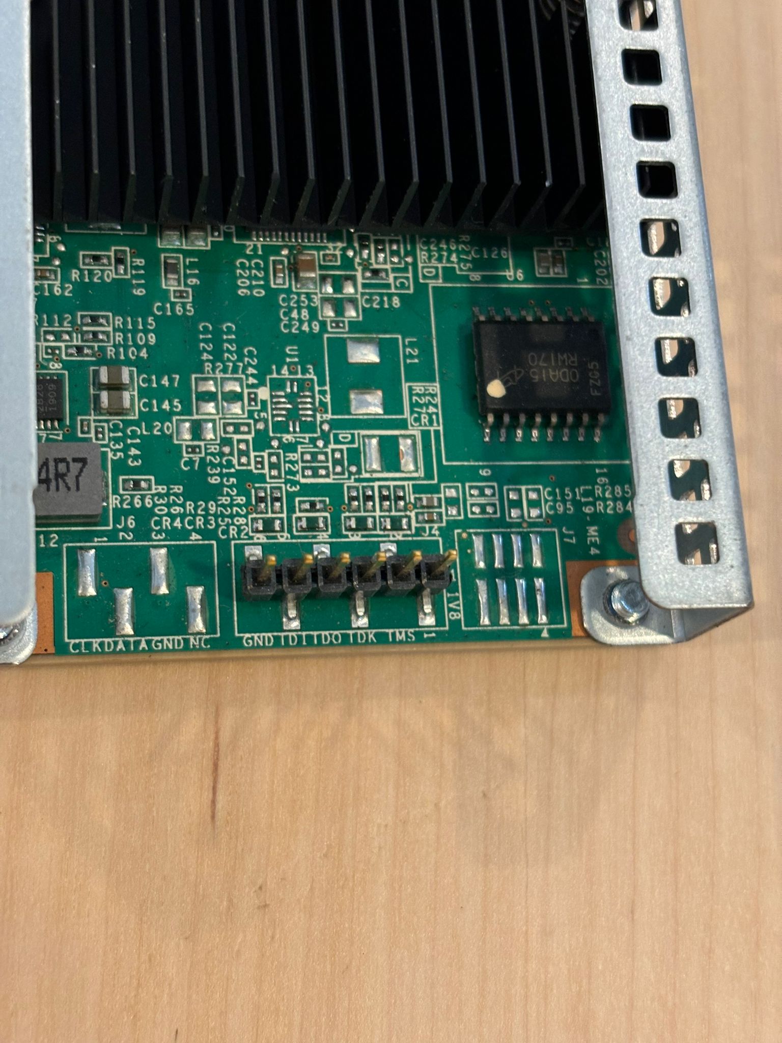
As for the width of x1, that is expected since the Broadcom bridge is also only x1 wide, and our board’s other 7 PCIe lanes are literally hanging over the side.
 7 PCIe lanes left unconnected and hanging over the air
Thus, we can finally confirm that this is our board and that the PCIe interface is working. We can now proceed to establishing the JTAG connection.
JTAG interface#
Xilinx FPGAs can be configured by writing a bitstream to their internal CMOS Configuration Latches (CCL). CCL is SRAM memory and volatile, thus the configuration is re-done on every power cycle. For devices in the field this bitstream would be read from an external SPI memory during initialization, or written from an external device, such as an embedded controller. But for development purposes overwriting the contents of the CCLs over JTAG is acceptable.
This configuration is done by shifting in the entire FPGA bitstream into the device’s configuration logic over the JTAG bus.
FPGA board JTAG interface#
As promised by the original eBay listing the board did come with an accessible JTAG interface, and gloriously enough, this time there wasn’t even the need for any additional soldering.
 View of the JTAG interface on the PCB
In addition to a power reference, and ground, conformely to the Xilinx JTAG interface it featured the four mandatory signals comprising the JTAG TAP :
- TCK Test Clock
- TMS Test Mode Select
- TDI Test Data Input
- TDO Test Data Output
Of note, the JTAG interface can also come with an independent reset signal. But since Xilinx JTAG interfaces do not have this independent reset signal, we be using the JTAG FSM reset state for our reset signal.
 6 pin board JTAG interface
This interface layout doesn’t follow a standard layout so I cannot just plug in one of my debug probes, it requires some re-wiring.
Segger JLINK :heart:#
I do not own an AMD approved JTAG programmer.
Traditionally speaking, the Segger JLink is used for debugging embedded CPUs let them be standalone or in a Zynq, and not for configuring FPGAs.
That said, all we need to do is use JTAG to shift in a bitstream to the CCLs, so technically speaking any programmable device with 4 sufficiently fast GPIOs can be used as a JTAG programmer. Additionally, the JLink is well supported by OpenOCD, the JLink’s libraries are open source, and I happened to own one.
Note : I could also have used a USB Blaster, which considering it is literally an Altera tool would have made it hilarious.
 20 pin segger JLink pinout
Wiring#
Rewiring :
 Wiring diagram to connect JLink JTAG probe to the board.
JTAG is a parallel protocol where TDI and TMS will be captured according to TCK. Because of this, good JTAG PCB trace length matching is advised in order to minimize skew.
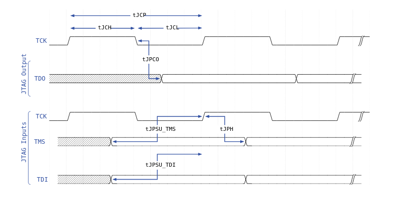 Timing Waveform for JTAG Signals (From Target Device Perspective); source : https://www.intel.com/content/www/us/en/docs/programmable/683719/current/jtag-timing-constraints-and-waveforms.html
Ideally a custom connector with length matched traces to work as an interface between the JLink’s probe and a board specific connector would be used.
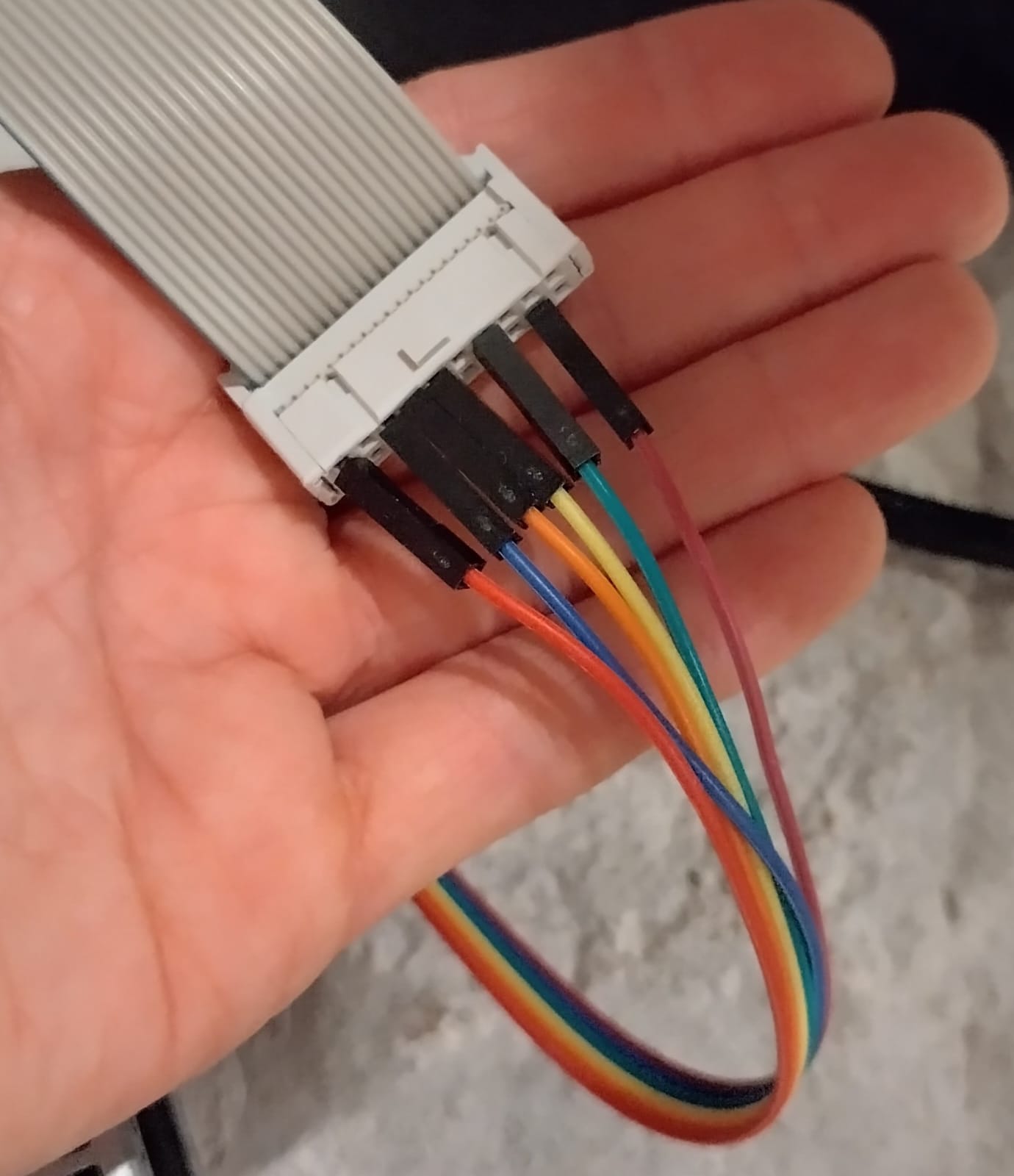 Far from length matched JTAG connections
Yet, here we are shoving breadboard wires between our debugger and the board. Since OpenOCD allows us to easily control the debugger clock speed, we can increase the skew tolerance by slowing down the TCK clock signal. As such there is no immediate need for a custom connector but we will not be able to reach the maximum JTAG speeds.
If no clock speed is specified OpenOCD sets the clock speed at 100MHz.
This is too high in our case.
As such, latter in the article, I will be setting the JTAG clock down to 1MHz for probing and reset, programming will be done at 10MHz.
No issues were encountered at these speeds.
OpenOCD#
OpenOCD is a free and open source on-chip debugger software that aims to be compatible with as many probes, boards and chips as possible.
Since OpenOCD has support for the standard SVF file format, my plan for my flashing flow will be to use Vivado to generate the SVF and have OpenOCD flash it. Now, some of you might be starting to notice that I am diverging quite far from the well lit path of officially supported tools. Not only am I using a not officially supported debug probe, but I am also using some obscure open source software with questionable support for interfacing with Xilinx UltraScale+ FPGAs. You might be wondering, given that the officially supported tools can already prove themselves to be a headache to get working properly, why am I seemingly making my life even harder?
The reason is quite simple: when things inevitably start going wrong, as they will, having an entirely open toolchain, allows me to have more visibility as to what is going on and the ability to fix it. I cannot delve into a black box.
Building OpenOCD#
By default the version of OpenOCD that I got on my server via the official packet manager was outdated and missing features I will need.
Also, since saving the ability to modify OpenOCD’s source code could come in handy, I decided to re-build it from source.
Thus, in the following logs, I will be running OpenOCD version 0.12.0+dev-02170-gfcff4b712.
Note : I have also re-build the JLink libs from source.
Determining the scan chain#
Since I do not have the schematics for the board I do not know how many devices are daisy-chainned on the board JTAG bus. Also, I want to confirm if the FPGA on the ebay listing is actually the one on the board. In JTAG, each chained device exposes an accessible IDCODE register used to identify the manufacturer, device type, and revision number.
When setting up the JTAG server, we typically define the scan chain by specifying the expected IDCODE for each TAP and the corresponding instruction register length, so that instructions can be correctly aligned and routed to the intended device. Given this is an undocumented board off Ebay, I do not know what the chain looks like. Fortunately, OpenOCD has an autoprobing functionality, to do a blind interrogation in an attempt to discover the available devices.
Thus, my first order of business was doing this autoprobing.
In OpenOCD the autoprobing is done when the configuration does not specify any taps.
The blind interrogation successfully discovered a single device on the chain with an IDCODE of 0x04a63093.
gp@workhorse:~/tools/openocd_jlink_test/autoprob$ openocd Open On-Chip Debugger 0.12.0+dev-02170-gfcff4b712 (2025-09-04-21:02) Licensed under GNU GPL v2 For bug reports, read http://openocd.org/doc/doxygen/bugs.html none separate Info : Listening on port 6666 for tcl connections Info : Listening on port 4444 for telnet connections Info : J-Link V10 compiled Jan 30 2023 11:28:07 Info : Hardware version: 10.10 Info : VTarget = 1.812 V Info : clock speed 1 kHz Warn : There are no enabled taps. AUTO PROBING MIGHT NOT WORK!! Info : JTAG tap: auto0.tap tap/device found: 0x04a63093 (mfg: 0x049 (Xilinx), part: 0x4a63, ver: 0x0) Warn : AUTO auto0.tap - use "jtag newtap auto0 tap -irlen 2 -expected-id 0x04a63093" Error: IR capture error at bit 2, saw 0x3ffffffffffffff5 not 0x...3 Warn : Bypassing JTAG setup events due to errors Warn : gdb services need one or more targets definedComparing against the UltraScale Architecture Configuration User Guide (UG570) we see that this IDCODE matches up precisely with the expected value for the KU3P.
 JTAG and IDCODE for UltraScale Architecture-based FPGAs
By default OpenOCD assumes a JTAG IR length of 2 bits, while our FPGA has an IR length of 6 bits. This is the cause behind the IR capture error encountered during autoprobing. By updating the script with an IR length of 6 bits we can re-detect the FPGA with no errors.
Output :
gp@workhorse:~/tools/openocd_jlink_test/autoprob$ openocd Open On-Chip Debugger 0.12.0+dev-02170-gfcff4b712 (2025-09-04-21:02) Licensed under GNU GPL v2 For bug reports, read http://openocd.org/doc/doxygen/bugs.html Info : Listening on port 6666 for tcl connections Info : Listening on port 4444 for telnet connections Info : J-Link V10 compiled Jan 30 2023 11:28:07 Info : Hardware version: 10.10 Info : VTarget = 1.812 V Info : clock speed 1 kHz Info : JTAG tap: auto_detect.tap tap/device found: 0x04a63093 (mfg: 0x049 (Xilinx), part: 0x4a63, ver: 0x0) Warn : gdb services need one or more targets definedBased on the probing, this is the JTAG scan chain for our board :
 JTAG scan chain for the alibaba cloud FPGA
System Monitor Registers#
Previous generations of Xilinx FPGA had a system called the XADC that, among other features, allowed you to acquire chip temperature and voltage readings. The newer UltraScale and UltraScale+ family have deprecated this XADC module in favor of the SYSMON (and SYSMON4) which allows you to also get these temperature readings, just better.
Unfortunately, openOCD didn’t have support for reading the SYSMON over JTAG out of the box, so I will be adding it.
To be more precise, the Kintex UltraScale+ has a SYSMON4 and not a SYSMON.
For full context, there are 3 flavors of SYSMON: For the purpose of this article, all these instances are similar enough that I will be using the terms SYSMON4 and SYSMON interchangeably.
Yes, you read that correctly the Zynq of the UltraScale+ series features not one, but at least two unique SYSMON instances.
In order for the JTAG to interact with the SYSMON, we first need to write the SYSMON_DRP command to the JTAG Instruction Register (IR). Based on the documentation, we see that this command has a value of 0x37, which funnily enough, is the same command code as the XADC, solidifying the SYSMON as the XADC’s descendant.
The SYSMON offers a lot more additional functionalities than just being used to read voltage and temperature, but for today’s use case we will not be using any of that. Rather, we will focus only on reading a subset of the SYSMON status registers.
These status registers are located at addresses (00h-3Fh, 80h-BFh), and contain the measurement results of the analog-to-digital conversions, the flag registers, and the calibration coefficients. We can select which address we wish to read by writing the address to the Data Register (DR) over JTAG and the data will be read out of TDO.
I added a report that reads the current chip temperature, internal and external voltages as well as the maximum values for these recorded since FPGA power cycle, to my flashing script output:
gp@workhorse:~/tools/openocd_jlink_test$ openocd Open On-Chip Debugger 0.12.0+dev-02170-gfcff4b712 (2025-09-04-20:02) Licensed under GNU GPL v2 For bug reports, read http://openocd.org/doc/doxygen/bugs.html set chipname XCKU3P Read temperature sysmon 4 Info : J-Link V10 compiled Jan 30 2023 11:28:07 Info : Hardware version: 10.10 Info : VTarget = 1.819 V Info : clock speed 1 kHz Info : JTAG tap: XCKU3P.tap tap/device found: 0x04a63093 (mfg: 0x049 (Xilinx), part: 0x4a63, ver: 0x0) Warn : gdb services need one or more targets defined -------------------- Sysmon status report : TEMP 31.12 C MAXTEMP 34.62 C VCCINT 0.852 V MAXVCC 0.855 V VCCAUX 1.805 V MAXVCCAUX 1.807 VPinout#
To my indescribable joy I happened to stumble onto this gold mine, in which we get the board pinout. This most likely fell off a truck: https://blog.csdn.net/qq_37650251/article/details/145716953
So far this pinout looks correct.
| 0 | diff_100mhz_clk_p | LVDS | E18 | BANK67 |
| 1 | diff_100mhz_clk_n | LVDS | D18 | BANK67 |
| 2 | sfp_mgt_clk_p | LVDS | K7 | BANK227 |
| 3 | sfp_mgt_clk_n | LVDS | K6 | BANK227 |
| 4 | sfp_1_txn | - | B6 | BANK227 |
| 5 | sfp_1_txp | - | B7 | BANK227 |
| 6 | sfp_1_rxn | - | A3 | BANK227 |
| 7 | sfp_1_rxp | - | A4 | BANK227 |
| 8 | sfp_2_txn | - | D6 | BANK227 |
| 9 | sfp_2_txp | - | D7 | BANK227 |
| 10 | sfp_2_rxn | - | B1 | BANK227 |
| 11 | sfp_2_rxp | - | B2 | BANK227 |
| 12 | SFP_1_MOD_DEF_0 | LVCMOS18 | D14 | BANK87 |
| 13 | SFP_1_TX_FAULT | LVCMOS18 | B14 | BANK87 |
| 14 | SFP_1_LOS | LVCMOS18 | D13 | BANK87 |
| 15 | SFP_1_LED | LVCMOS18 | B12 | BANK87 |
| 16 | SFP_2_MOD_DEF_0 | LVCMOS18 | E11 | BANK86 |
| 17 | SFP_2_TX_FAULT | LVCMOS18 | F9 | BANK86 |
| 18 | SFP_2_LOS | LVCMOS18 | E10 | BANK86 |
| 19 | SFP_2_LED | LVCMOS18 | C12 | BANK87 |
| 20 | IIC_SDA_SFP_1 | LVCMOS18 | C14 | BANK87 |
| 21 | IIC_SCL_SFP_1 | LVCMOS18 | C13 | BANK87 |
| 22 | IIC_SDA_SFP_2 | LVCMOS18 | D11 | BANK86 |
| 23 | IIC_SCL_SFP_2 | LVCMOS18 | D10 | BANK86 |
| 24 | IIC_SDA_EEPROM_0 | LVCMOS18 | G10 | BANK86 |
| 25 | IIC_SCL_EEPROM_0 | LVCMOS18 | G9 | BANK86 |
| 26 | IIC_SDA_EEPROM_1 | LVCMOS18 | J15 | BANK87 |
| 27 | IIC_SCL_EEPROM_1 | LVCMOS18 | J14 | BANK87 |
| 28 | GPIO_LED_R | LVCMOS18 | A13 | BANK87 |
| 29 | GPIO_LED_G | LVCMOS18 | A12 | BANK87 |
| 30 | GPIO_LED_H | LVCMOS18 | B9 | BANK86 |
| 31 | GPIO_LED_1 | LVCMOS18 | B11 | BANK86 |
| 32 | GPIO_LED_2 | LVCMOS18 | C11 | BANK86 |
| 33 | GPIO_LED_3 | LVCMOS18 | A10 | BANK86 |
| 34 | GPIO_LED_4 | LVCMOS18 | B10 | BANK86 |
| 35 | pcie_mgt_clkn | - | T6 | BANK225 |
| 36 | pcie_mgt_clkp | - | T7 | BANK225 |
| 37 | pcie_tx0_n | - | R4 | BANK225 |
| 38 | pcie_tx1_n | - | U4 | BANK225 |
| 39 | pcie_tx2_n | - | W4 | BANK225 |
| 40 | pcie_tx3_n | - | AA4 | BANK225 |
| 41 | pcie_tx4_n | - | AC4 | BANK224 |
| 42 | pcie_tx5_n | - | AD6 | BANK224 |
| 43 | pcie_tx6_n | - | AE8 | BANK224 |
| 44 | pcie_tx7_n | - | AF6 | BANK224 |
| 45 | pcie_rx0_n | - | P1 | BANK225 |
| 46 | pcie_rx1_n | - | T1 | BANK225 |
| 47 | pcie_rx2_n | - | V1 | BANK225 |
| 48 | pcie_rx3_n | - | Y1 | BANK225 |
| 49 | pcie_rx4_n | - | AB1 | BANK224 |
| 50 | pcie_rx5_n | - | AD1 | BANK224 |
| 51 | pcie_rx6_n | - | AE3 | BANK224 |
| 52 | pcie_rx7_n | - | AF1 | BANK224 |
| 53 | pcie_tx0_p | - | R5 | BANK225 |
| 54 | pcie_tx1_p | - | U5 | BANK225 |
| 55 | pcie_tx2_p | - | W5 | BANK225 |
| 56 | pcie_tx3_p | - | AA5 | BANK225 |
| 57 | pcie_tx4_p | - | AC5 | BANK224 |
| 58 | pcie_tx5_p | - | AD7 | BANK224 |
| 59 | pcie_tx6_p | - | AE9 | BANK224 |
| 60 | pcie_tx7_p | - | AF7 | BANK224 |
| 61 | pcie_rx0_p | - | P2 | BANK225 |
| 62 | pcie_rx1_p | - | T2 | BANK225 |
| 63 | pcie_rx2_p | - | V2 | BANK225 |
| 64 | pcie_rx3_p | - | Y2 | BANK225 |
| 65 | pcie_rx4_p | - | AB2 | BANK224 |
| 66 | pcie_rx5_p | - | AD2 | BANK224 |
| 67 | pcie_rx6_p | - | AE4 | BANK224 |
| 68 | pcie_rx7_p | - | AF2 | BANK224 |
| 69 | pcie_perstn_rst | LVCMOS18 | A9 | BANK86 |
Global clock#
On high end FPGAs like the UltraScale+ family, high-speed global clocks are typically driven from external sources using differential pairs for better signal integrity.
According to the pinout we have two such differential pairs.
First I must determine the nature of these external reference clocks to see how I can use them to drive my clocks.
These differential pairs are provided over the following pins:
- 100MHz : {E18, D18}
- 156.25MHz : {K7, K6}
Judging by the naming and the frequencies, the 156.25MHz clock is likely my SFP reference clock, and the 100MHz can be used as my global clock.
We can confirm by querying the pin properties.
K6 properties :
E18 properties :
This tells us:
- The differential pairings are correct: {K6, K7}, {E18, D18}
- We can easily use the 100MHz as a source to drive our global clocking network
- The 156.25MHz clock is to be used as the reference clock for our GTY transceivers and lands on bank 227 as indicated by the PIN_FUNC property MGTREFCLK0N_227
- We cannot directly use the 156.25MHz clock to drive our global clock network
With all this we have sufficient information to write a constraint file (xdc) for this board.
Test design#
Further sections will be using the following design files.
top.v:
alibaba_cloud.xdc :
Writing the bitstream#
My personal belief is that one of the most important contributors to design quality is iteration cost. The lower your iteration cost, the higher your design quality is going to be.
As such I will invest the small upfront cost to have the workflow be as streamlined as efficiently feasible.
Thus, my workflow evolved into doing practically everything over the command line interfaces and only interacting with the tools, Vivado in this case, through tcl scripts.
Vivado flow#
The goal of this flow is to, given a few verilog design and constraint files produce a SVF file. Our steps are :
- creat the Vivado project setup.tcl
- run the implementation build.tcl
- generate the bitstream and the SVF gen.tcl
I will be using make to kick off and manage the dependencies between the different steps, though I recognise this isn’t a widespread practice for hardware projects. make is a highly flexible, reliable and powerful tool and I believe its ability to tie together any type of workflow makes it a prime tool for this use case.
We will be invoking Vivado in batch mode, this allows us to provide a tcl script alongside script arguments, the format is as following :
Though this allows us to easily break down our flow into incremental stages, invoking a single script in batch mode has the drawback of restarting Vivado and needing to re-load the project or the project checkpoint on each invocation.
As the project size grows so will the project load time, so segmenting the flow into a large number of independent scripts comes at an increasing cost.
Makefile :
setup.tcl :
build.tcl :
Generating the SVF file#
The SVF for Serial Vector Format is a human readable, vendor agnostic specification used to specify JTAG bus operations.
Example SVF file, test program:
! Initialize UUT STATE RESET; ! End IR scans in DRPAUSE ENDIR DRPAUSE; ! End DR scans in DRPAUSE ENDDR DRPAUSE; ! 24 bit IR header HIR 24 TDI (FFFFFF); ! 3 bit DR header HDR 3 TDI (7); ! 16 bit IR trailer TIR 16 TDI (FFFF); ! 2 bit DR trailer TDR 2 TDI (3); ! 8 bit IR scan, load BIST opcode SIR 8 TDI (41) TDO (81) MASK (FF); ! 16 bit DR scan, load BIST seed SDR 16 TDI (ABCD); ! RUNBIST for 95 TCK Clocks RUNTEST 95 TCK ENDSTATE IRPAUSE; ! 16 bit DR scan, check BIST status SDR 16 TDI (0000) TDO(1234) MASK(FFFF); ! Enter Test-Logic-Reset STATE RESET; ! End Test ProgramVivado can generate a hardware aware SVF file containing the configuration sequence for an FPGA board, allowing us to write a bitstream.
Given the SVF file literally contains the bitstream written in clear hexademical, in the file, our first step is to generate our design’s bitstream.
Vivado proper isn’t the software that generates the SVF file, this task is done by the hardware manager which handles all of the configuration.
We can launch a new instance open_hw_manager and connect to it connect_hw_server. Since JTAG is a daisy chained bus, and given the SVF file is just a standardised way of specifying JTAG bus operations, in order to generate a correct JTAG configuration sequence, we must inform the hardware manger of our scan chain.
During our earlier probing of the scan chain, we have established that our FPGA is the only device on the chain. We inform the hardware manager of this by creating a new device configuration ( the term “device” refers to the “board” here ) and add our fpga to the chain using the create_hw_device -part <device name>.When we have multiple devices we should register them following the order in which they appear on the chain.
Finally to generate the SVF file, we must select the device we wish to program with program_hw_device <hw_device>, then write out the SVF to the file using write_hw_svf <path to svf file>.
gen.tcl:
Configuring the FPGA using OpenOCD#
Although not widespread openOCD has a very nice svf execution command :
18.1 SVF: Serial Vector Format#
The Serial Vector Format, better known as SVF, is a way to represent JTAG test patterns in text files. In a debug session using JTAG for its transport protocol, OpenOCD supports running such test files.
[Command]svf filename [-tap tapname] [[-]quiet] [[-]nil] [[-]progress] [[-]ignore_error]This issues a JTAG reset (Test-Logic-Reset) and then runs the SVF script from filename. Arguments can be specified in any order; the optional dash doesn’t affect their se- mantics.
Command options:
- -tap tapname ignore IR and DR headers and footers specified by the SVF file with HIR, TIR, HDR and TDR commands; instead, calculate them automatically according to the current JTAG chain configuration, targeting tapname;
- [-]quiet do not log every command before execution;
- [-]nil “dry run”, i.e., do not perform any operations on the real interface;
- [-]progress enable progress indication;
- [-]ignore_error continue execution despite TDO check errors.
We invoke it in our openOCD script using the -progress option for additional logging.
openocd :
Flashing sequence log :
gp@workhorse:~/tools/openocd_jlink_test$ openocd Open On-Chip Debugger 0.12.0+dev-02170-gfcff4b712 (2025-09-04-21:02) Licensed under GNU GPL v2 For bug reports, read http://openocd.org/doc/doxygen/bugs.html set chipname XCKU3P Read temperature sysmon 4 Info : J-Link V10 compiled Jan 30 2023 11:28:07 Info : Hardware version: 10.10 Info : VTarget = 1.812 V Info : clock speed 1 kHz Info : JTAG tap: XCKU3P.tap tap/device found: 0x04a63093 (mfg: 0x049 (Xilinx), part: 0x4a63, ver: 0x0) Warn : gdb services need one or more targets defined -------------------- Sysmon status report : TEMP 50.46 C MAXTEMP 52.79 C VCCINT 0.846 V MAXVCC 0.860 V VCCAUX 1.799 V MAXVCCAUX 1.809 V -------------------- svf processing file: "out/project_prj_checkpoint.svf" 0% TRST OFF; 0% ENDIR IDLE; 0% ENDDR IDLE; 0% STATE RESET; 0% STATE IDLE; 0% FREQUENCY 1.00E+07 HZ; adapter speed: 10000 kHz 0% HIR 0 ; 0% TIR 0 ; 0% HDR 0 ; 0% TDR 0 ; 0% SIR 6 TDI (09) ; 0% SDR 32 TDI (00000000) TDO (04a63093) MASK (0fffffff) ; 0% STATE RESET; 0% STATE IDLE; 0% SIR 6 TDI (0b) ; 0% SIR 6 TDI (14) ; 0% RUNTEST 0.100000 SEC; 0% RUNTEST 10000 TCK; 0% SIR 6 TDI (14) TDO (11) MASK (31) ; 0% SIR 6 TDI (05) ; 95% ffffffffffff) ; 95% SIR 6 TDI (09) TDO (31) MASK (11) ; 95% STATE RESET; 95% RUNTEST 5 TCK; 95% SIR 6 TDI (05) ; 95% SDR 160 TDI (0000000400000004800700140000000466aa9955) ; 95% SIR 6 TDI (04) ; 95% SDR 32 TDI (00000000) TDO (3f5e0d40) MASK (08000000) ; 95% STATE RESET; 95% RUNTEST 5 TCK; Info : Listening on port 6666 for tcl connections Info : Listening on port 4444 for telnet connectionsResulting in a successfully configured our FPGA.
Conclusion#
For $200 we got a fully working decommissioned Alibaba Cloud accelerator featuring a Kintex UltraScale+ FPGA with an easily accessible debugging/programming interface and enough pinout information to define our own constraint files.
We also have a fully automated Vivado workflow to implement our designs and the ability to write the bitstream, and interface with the FPGA’s internal JTAG accessible registers using an open source programming tool without the need for an official Xilinx programmer.
In the end, this project delivered an at least 5x cost savings over commercial boards (compared to the lowest cost $900-1050 Alinx alternatives), making this perhaps the most cost effective entry point for a Kintex UltraScale+ board.
External ressources#
Xilinx Vivado Supported Devices : https://docs.amd.com/r/en-US/ug973-vivado-release-notes-install-license/Supported-Devices
Official Xilinx dev board : https://www.amd.com/en/products/adaptive-socs-and-fpgas/evaluation-boards/ek-u1-kcu116-g.html
Alinx Kintex UltraScale+ dev boards : https://www.en.alinx.com/Product/FPGA-Development-Boards/Kintex-UltraScale-plus.html
UltraScale Architecture Configuration User Guide (UG570) : https://docs.amd.com/r/en-US/ug570-ultrascale-configuration/Device-Resources-and-Configuration-Bitstream-Lengths?section=gyn1703168518425__table_vyh_4hs_szb
UltraScale Architecture System Monitor User Guide (UG580): https://docs.amd.com/v/u/en-US/ug580-ultrascale-sysmon
Vivado Design Suite Tcl Command Reference Guide (UG835): https://docs.amd.com/r/en-US/ug835-vivado-tcl-commands/Tcl-Initialization-Scripts
PCI vendor/device ID database: https://admin.pci-ids.ucw.cz/read/PC/14e4
PCI device classes: https://admin.pci-ids.ucw.cz/read/PD
Linux kernel PCI IDs: https://github.com/torvalds/linux/blob/7aac71907bdea16e2754a782b9d9155449a9d49d/include/linux/pci_ids.h#L160-L3256
Linux kernel PCI classes: https://github.com/torvalds/linux/blob/7aac71907bdea16e2754a782b9d9155449a9d49d/include/linux/pci_ids.h#L15-L158
Truck-kun pinout: https://blog.csdn.net/qq_37650251/article/details/145716953
Ebay listing: https://www.ebay.com/itm/167626831054?_trksid=p4375194.c101800.m5481
OpenOCD documentation: https://openocd.org/doc-release/pdf/openocd.pdf