Table of Contents:
Part-1 : So what is digital logic design exactly?
Part-2 : Using structural Verilog to make a working FPGA design.
Part-3 : Using RTL Verilog and HDL to infer a working FPGA design.
Part-4 : The magic of LUTs to implement random logic in an FPGA.
Part-5 : Digital Logic Simulation at the RTL level using ModelSim.
Part-6 : Digital Logic Simulation at the RTL level using VivadoSim.
Part-7 : Design hierarchy and the ChipVault IDE.
Part-8 : Finite State Machines.
Part-9 : Timing Closure.
Part-10 : Placement and Floorplanning.
Part-11 : IO Banks.
Part-12 : RAMs and ROMs.
Part-13 : FIFOs
Part-14 : Clocking
Part-15 : Digital Logic Simulation
Part-16 : Test Benches
2025.06.30 : Quick update, this blog series is now a complete book!
Click on this link for my book Mastering FPGA Chip Design : For Speed, Area, Power, and Reliability published by Elektor Publishing in their “Academy Pro” series of electronic books.
PodCast interview on YouTube :
2024.05.18 : I’m Kevin Hubbard, BSEE. It’s hard to believe ( and I constantly pinch myself ), but I’ve been designing with digital logic for 45 years now. I got started as a 1980’s Radio Shack kid, scrounging dollar bills to buy the latest TTL logic chips in DIP packages like the 7400 series ( 7474, 74244, 74245, 74373, 74374, etc ). I built little digital interfaces for my 8bit 6502 Apple ][+ and Z80 TRS-80 Model-1 computers of that era. Everything back then was 1 MHz at 5V. Very forgiving to breadboards, long wires and missing bypass caps ( what are those? ).
My hobbyist passion for electronics steered me to surviving high school and getting a BSEE degree in the early 1990’s from the University of Washington. Zero engineering in the family, but I knew this was what I wanted to do. My career ambitions as a child was either electronics or become a professional LEGO builder. Get this, after graduation companies actually paid me to design digital PCBs, FPGAs and ASICs in the electronics industry. Still pinching myself on that. Also still enjoy building with LEGOs ( without pay ).

30+ years later, my career is not quite sunsetting, but I’ve decided it’s a great time to start sharing a little knowledge learned along my journey in electroincs. I’ve seen things you people wouldn’t believe. 22V10 PALs with only 10 flip-flops costing 10s of dollars transition to Xilinx 4036XLs making the seemingly impossible possible. I watched CMOS Voh/Vih levels drop rapidly from 5V to 1.2V. All those moments will be lost in time, like tears in rain. Time to share some of my knowledge of CMOS digital logic design.
I’m planning a multi-part ( 1ofN ) FPGA design series that starts out super simple ( flashing a “Hello World” LED at 1 Hz ) and gradually move up to a simple VGA graphics “GPU” with an embedded OSH Sump3 ILA logic analyzer for analyzing VGA timing live and interfacing over USB to a Python GUI application running on a PC. I’d like to end with a simple SPI interface to give an RP2040 uC running CircuitPython some cool VGA graphics – TBD. Far too many people think FPGAs are somehow like microcontrollers and designing Verilog/VHDL RTL is somehow the same as software “computer programming”. I wish to enlighten them.
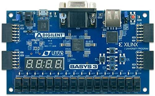
After long and careful consideration, the FPGA Dev Board I selected for this tutorial project is the “BASYS 3” from Digilent. It’s readily available from Amazon ( here ) – making it much easier to acquire than other FPGA dev boards.
So why this board in particular? It has a couple of key features :
- Reasonable price at $165. Cheap enough for a person to buy. I’m not really a fan of the $500 to $1,000 boards out there.
- Modern (28nm) Artix-7 FPGA that is targetable using the latest free version of AMD / Xilinx Vivado design software.
- Built in FTDI USB interface. All of my Python software to FPGA projects use an FTDI FT232 cable, so this interface built in is a key feature.
- Simple RGB 4-4-4 analog VGA graphics. Monitors with VGA inputs are still around – so why bother with the TMDS complexity of HDMI graphics? VGA is “good enough” still for some things.
- Flexible configuration interface. This board has a unique PIC microcontroller that will read a “top.bit” file from a USB “thumb drive” and configure the FPGA from it.
That last feature closed the deal for me. Simply being able to drop a bitfile onto a USB stick and configure the FPGA from it is a fantastic feature. I develop in a 99% Linux environment and JTAG configuration from Linux has always been problematic. JTAG programming cables can also be expensive ( although this board has an “HS2” compatible one built in as well ). I use low cost 2:1 USB switches like this for sharing a single USB “thumb drive” between multiple host computers ( like a desktop and an oscilloscope ).
Want to join along?
Step-1 : Buy the board.
Step-2 : Download the free Vivado software from AMD / Xilinx website here. I will be using Vivado v2022.2 running on Linux. Which version or platform you use really shouldn’t matter though so long as the Artix7 XC7A35T device is supported.
Step-3 : Start reading along and come back on a regular basis as I post new chapters to the series.
So let’s get started with this FPGA Tutorial from Black Mesa Labs. This quick intro was Part-0.
Part-1, So what is digital logic design exactly?
.png)


