.png)

 ITT 2025 Chandler Fab Tour 5 Large
Last week, I had the opportunity to tour a part of Intel Fab 52 in Chandler, Arizona. This is only 35 minutes or so from the STH studio. If you do not know this, Phoenix, Arizona, is becoming a hotbed for semiconductor manufacturing in the US. Intel has had manufacturing operations roughly 30 minutes south of Phoenix in Chandler for decades. TSMC is building its leading-edge US facilities roughly 30 minutes north of Phoenix. At Semicon West 2025 this week, a lot of badges were from Arizona. Intel, for its part, is manufacturing its next-generation Panther Lake and Clearwater Forest chips in its new 18A process, and doing it at Fab 52 in Arizona.
Intel Fab 52 in Chandler, Arizona, is Running 18A
Intel 18A is a big bet for Intel, to say the least. The two big new features are the RibbonFET and PowerVia technologies.
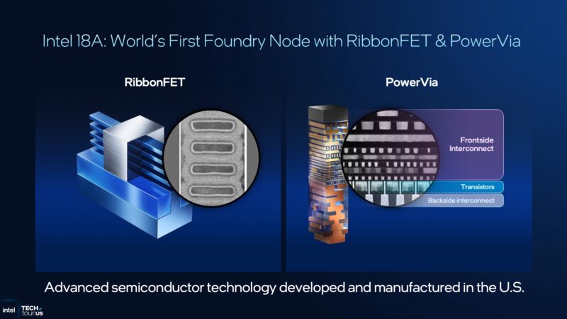 ITT 2025 Intel Opening Keynote Intel 18A RibbonFET And PowerVIA 2
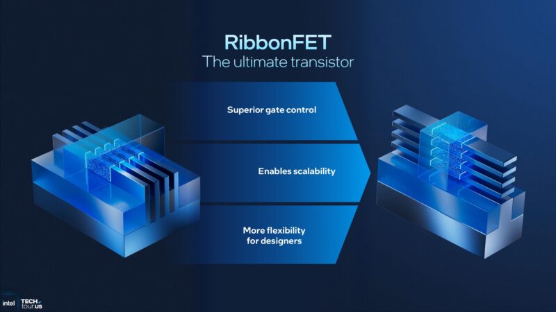
RibbonFET is the next-generation of transistor. Aside from the feature size which has an, at best, fuzzy correlation with process names, a major benefit of these new process technologies is also transistor designs that intercept new process node inflection points.
 ITT 2025 Intel Opening Keynote Intel 18A RibbonFET 2
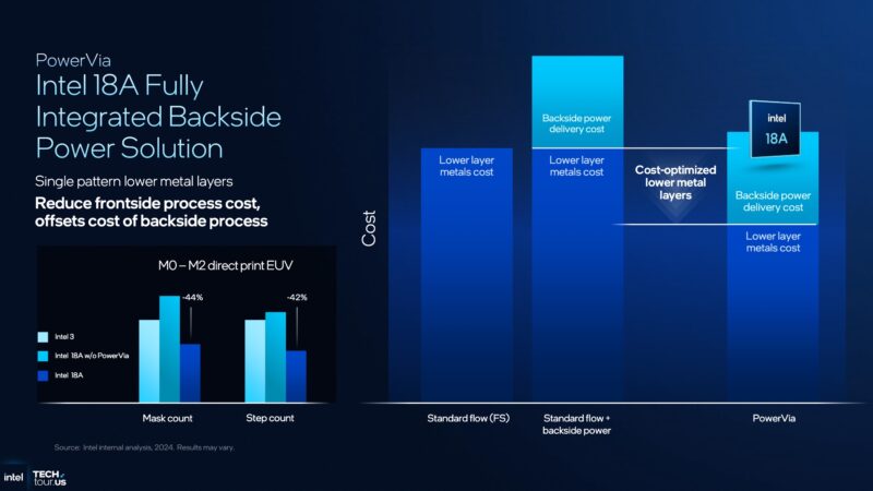
PowerVia adds backside power delivery. Instead of having power and signal wires intertwined where interference from the power wires both from a physical and electrical standpoint can be a challenge, PowerVia moves the power delivery to the other side of the chip.
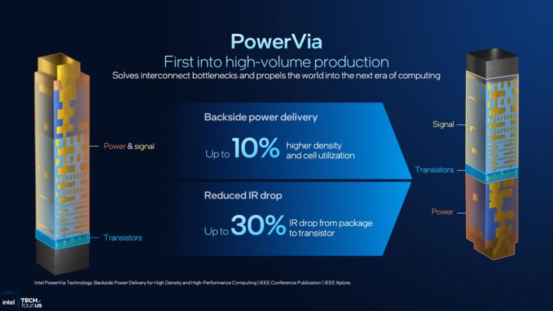 ITT 2025 Intel Opening Keynote Intel 18A PowerVIA 2
Normally, this would cost more to add to a design, but Intel says it is able to reap the benefits of backside power delivery at a relatively small cost adder because it lowers the material costs for the lower layers.
 ITT 2025 Intel Opening Keynote Intel 18A Backside Power 2
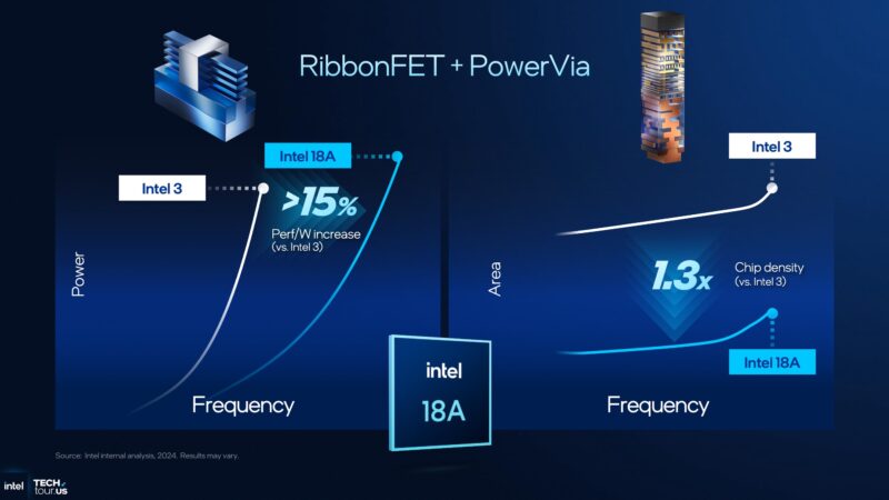
Intel says it can get a greater than 15% performance per watt increase over Intel 3 and better density.
 ITT 2025 Intel Opening Keynote Intel 18A RibbonFET And PowerVia Benefits 1 2
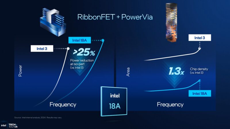
Alternatively, Intel says it can get 25% lower power at the same performance using these technologies. To be clear, there are many folks asking about Foundry customers for 18A, but for Intel Products at least, this has to be awesome as it is the first time in many years that Intel has had leadership process in high-volume production. Or better said, these are the types of innovations that help Intel Products teams show they have an advantage in high-value compute tiles. Of course, in modern heterogeneous SoCs, there are usually benefits to using older and less dense process nodes for IP like I/O chiplets. For compute, this is what you would want.
 ITT 2025 Intel Opening Keynote Intel 18A RibbonFET And PowerVia Benefits 2 2
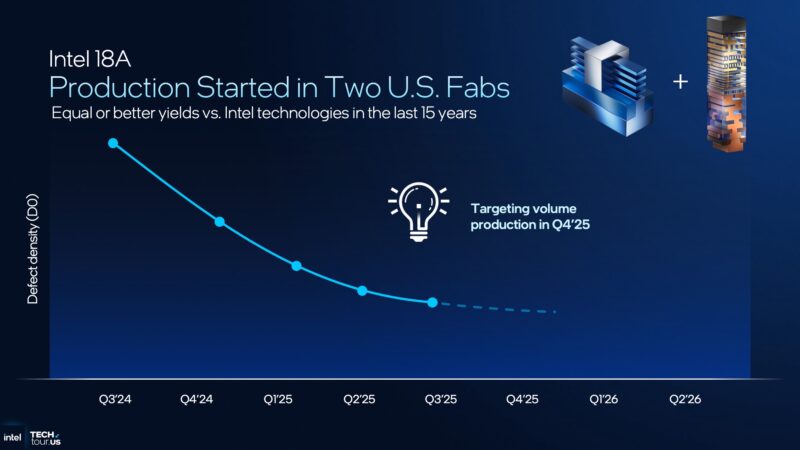
Intel also mentions that it is in production and is at equal or better yields compared to previous process nodes.
 ITT 2025 Intel Opening Keynote Intel 18A At Two US Fabs 2
A big part of that is enabled by the ASML machines. This may look small at first, but it is huge. We could not take a picture with a “banana for scale”, nor take photos inside the fab, but Intel was keen on showing this working and running wafers. Something to also keep in mind is that this is one level of the machine. Semiconductor manufacturing equipment usually has a large footprint not just like you would see here, but also on level(s) below the floor that this shot was taken from.
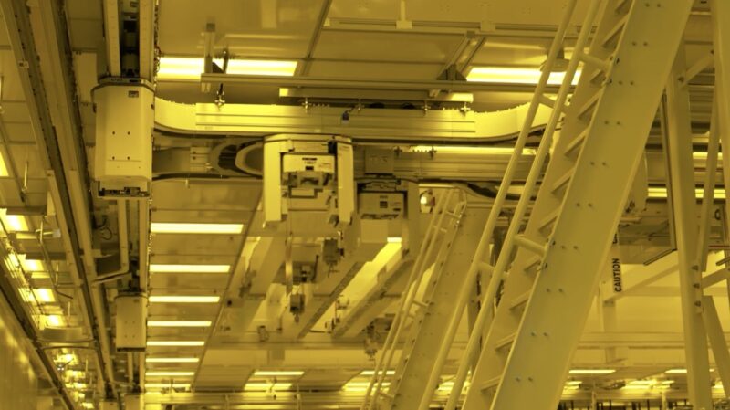
 ITT 2025 Chandler Fab Tour 6 Large
We actually were able to walk through Fab 42 after getting into our bunny suits en route to Fab 52. Machines were there from the well-known semiconductor equipment manufacturers and there was a lot running.
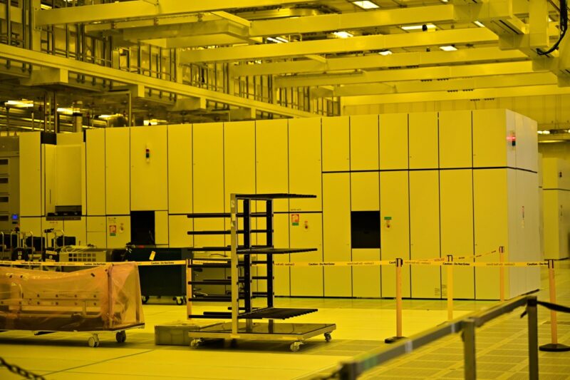
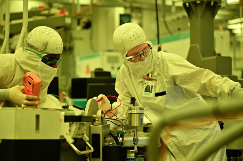
 ITT 2025 Chandler Fab Tour 1 Large
I know we have a number of folks who are older and remember the old Intel bunny suits from the 1990s when companies tried to remove all dust from the entire fab building. That was a challenge since the fab building had an enormous volume. Instead, wafers are transported in sealed carriers and the clean environments then becomes the insides of the carriers and machines. The rest of the fab still has a massive air filtration operation that you can feel walking through it, but the wafers and tools are actually kept clean in a different manner.
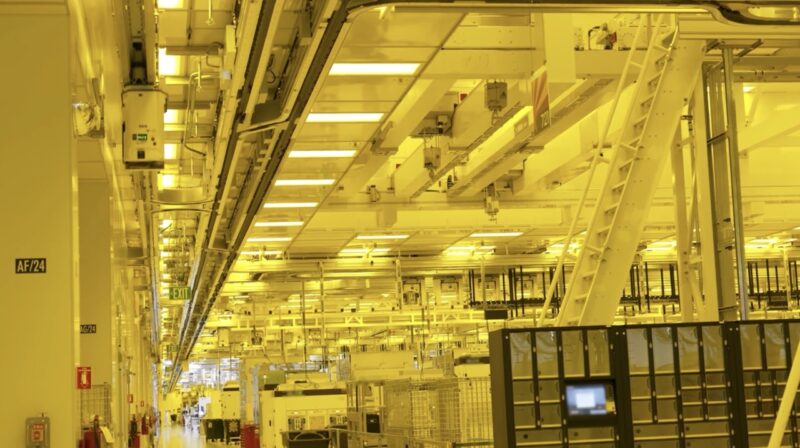
 ITT 2025 Inside Intel Chandler AZ Fab 1 Large
You also do not see folks walking around with wafers in the fabs, despite many press photos you might see. Instead, there are robots on the ceiling that run in tracks. They then drop down the wafer canisters with four wires.
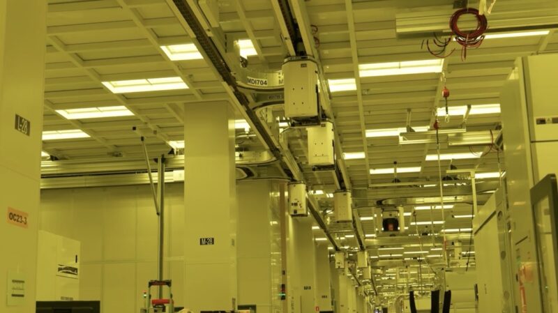 ITT 2025 Inside Intel Chandler AZ Fab 2 Large
If you have seen Sci Fi movies or some drone delivery services where the drone stays at altitude then drops the packages, this looks like that.
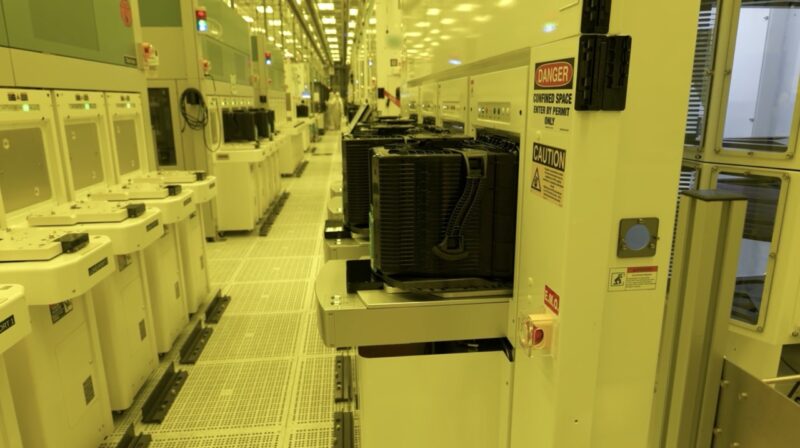
 ITT 2025 Inside Intel Chandler AZ Fab 4 Large
Because wafers arrive via this overhead system, tools are placed quite close together, but then the scale of the building is massive.
 ITT 2025 Inside Intel Chandler AZ Fab 5 Large
Something else that is striking is that when you think of manufacturing small client chips like Panther Lake, or plam sized chips like Clearwater Forest, and on thin 300mm wafers at some point it hits you the scale. You are in a huge building to manufacture microscopic sand art with some of the most precise tools that humanity has ever made.
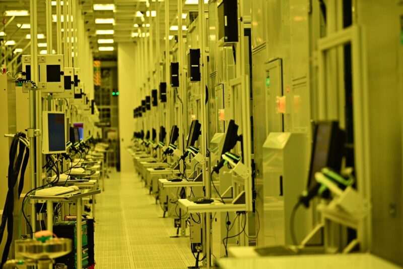
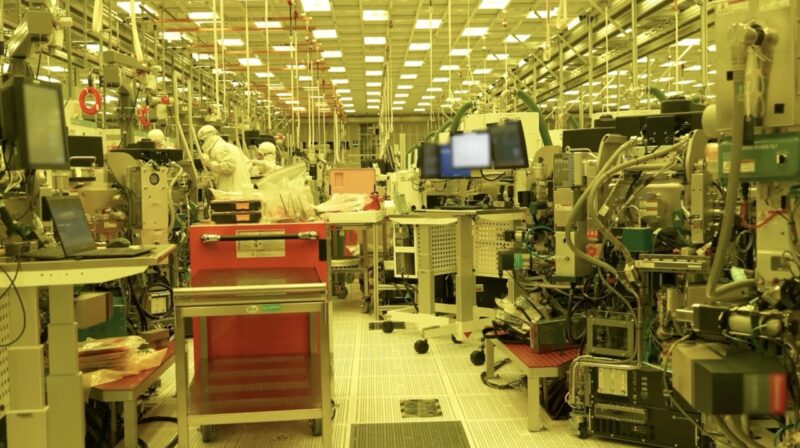 ITT 2025 Inside Intel Chandler AZ Fab 3 Large
The overall process is highly automated to say the least, but there are tons of folks working in the fabs.
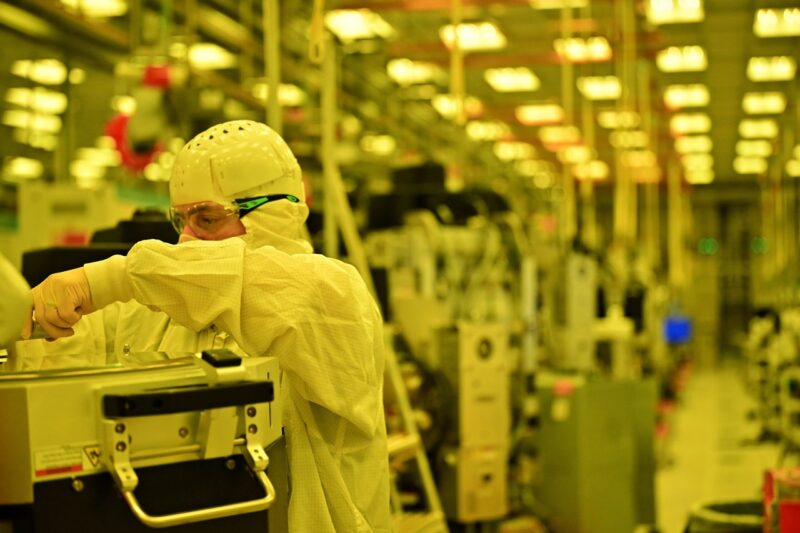 ITT 2025 Chandler Fab Tour 3 Large
A lot of these folks are working to maintain the machines. For folks who have never experienced this before, when folks say jobs at the fab, instead of the mental model of a cobbler making shoes to a fab worker making chips, it is more like the fab worker is making sure the cobbler’s tools are operating well.
 ITT 2025 Chandler Fab Tour 4 Large
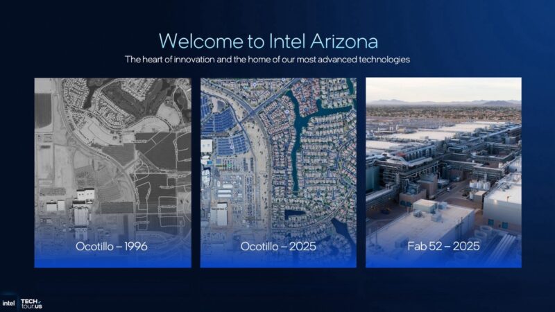
Another interesting one, especially now that we live in the area, is just the exterior of the building. Intel shared this Ocotillo 1996 to 2025 29 year overhead comparison. Farm land has given way to fabs and homes. Chandler, Arizona had under 10,000 residents in 1960. It is now roughly 300,000 residents. Intel bought the land decades ago and a reason to start building here is the same reason that Phoenix has become a major data center hub, first for banks and financial institutions, then for others. It is a relatively short haul to Los Angeles, and yet the area does not have hurricanes, tornados, tsunami threats, volcanic activity, or earthquakes. When we did the PhoenixNAP Data Center tour years ago, the reasons to put data centers here is similar to the reason you might want to put fabs here.
 ITT 2025 Intel Opening Keynote Intel Arizona 1996 To 2025 Large
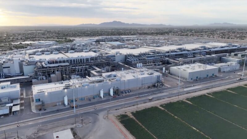
A few other observations. First, the fab itself is huge. You can see in the photos below just how big these buildings are. They are several stories not just in volume, but have several floors in each.
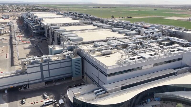
 ITT 2025 Outside Intel Chandler AZ Fab 4 Large
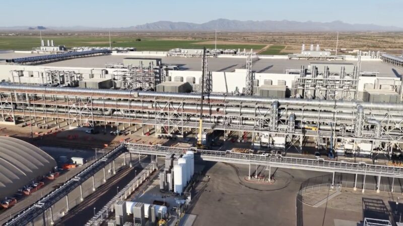
They also have a massive amount of specialized infrastructure investment around them.
 ITT 2025 Outside Intel Chandler AZ Fab 3 Large
If you were to drive north an hour or so, the desert in north Phoenix is being transformed by TSMC. TSMC’s campus looks quite a bit different but is no less impressive.
 ITT 2025 Outside Intel Chandler AZ Fab 2 Large
Another interesting aside, that I had no clue about before moving here is the water situation in Phoenix. Pre-1950 or so, this was desert. After various canal and aqueduct projects in the post WW2 era, Phoenix got water to turn the desert into farmland. Part of the reason Phoenix has shot from a few thousand poeple to the 5th largest city in the US over the span of a few decades is that water is being used much more efficiently. It turns out single family homes use a lot less water than the farmland they replaced, and so the population has grown at a crazy pace while water usage has not spiked.
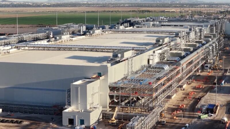
 ITT 2025 Outside Intel Chandler AZ Fab 1 Large
While one could point to the wastewater treatment and recycling plants for the fab, here is the other way to look at it. Arizona is built on the premise of thinking about water as a precious resource. In the photo above, you have Intel fabs manufacturing some of the world’s most advanced technology using water.
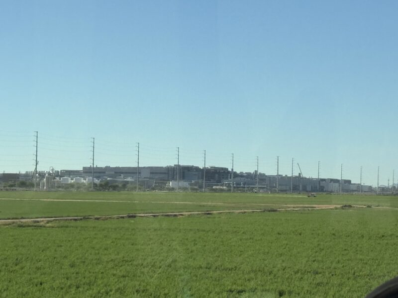 Intel Chandler Fabs From The Fields Large
You also can see fields of alfalfa being grown, likely as horse feed. Prior to moving to Arizona, I would have been in the camp of “where does the water come from?” After living here for two years, I find myself questioning whether the better use of our water is producing many jobs and high-tech products or growing horse feed. I am firmly in the build semiconductors and data centers camp as those are higher-value than hay.
Final Words
It was neat to go into the fabs and see modern manufacturing. Partly because this is where many of the product we review on STH are built. Also, just having moved here, it was neat to see one of the engines of the local economy. Especially having gone to Semicon West 2025 here after doing the fab tour, there are few things I am more certain of than the Phoenix area is set to build a lot of the world’s and the nation’s chips in the next few years.
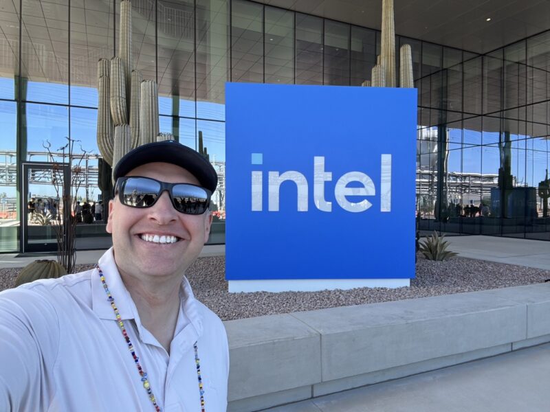 Patrick Intel Chandler Arizona Fab 2025 Large
There was certainly a bit of this trip that was Intel parading media and analysts in front of its ASML machines and saying “see we have 18A in production” which is fair. On the other hand, 18A brings a ton of innovation and a leadership process to Intel after many generations of not being able to say that. We are going to go into the products shortly, but this was great to see in-person.
![The Perfect Router Does Not Exi [video]](https://www.youtube.com/img/desktop/supported_browsers/firefox.png)