.png)

A few weeks ago I posted about how much fun I was having with the Fomu FPGA development board while travelling. This project from Tim ‘mithro’ Ansell and Sean ‘xobs’ Cross is not new, but remains a favorite of mine because of how portable it is — the entire board can fit in your USB port!
The Fomu includes a Lattice Semiconductor iCE40 UltraPlus 5K, which has been a popular FPGA option over the past few years due to the reverse engineered bitstream format and ability to program it with a fully open source toolchain (see updated repository here). One of the more recent production uses I have heard about is in the Oxide Computer, which I discussed with Nathanael Huffman on an episode of Microarch Club and has also come up on the Oxide & Friends podcast.
One of the most interesting attributes of the Fomu is that, despite the fact that it is programmed over USB, it doesn’t actually include any USB peripheral hardware. Instead, in order to make the board small enough to fit in the USB port, the USB core is implemented in RTL (Fomu uses ValentyUSB) and is included in the Foboot bootloader. Most FPGAs support writing bitstreams directly into SRAM, meaning that it will have to be reprogrammed after a power cycle, or storing a bistream in a separate flash IC that the FPGA will read from when powered on. iCE40 FPGAs are no different, but also include a Non-Volatile Configuration Memory (NVCM), which allows for one-time programming of a bitstream in high-volume applications. From the iCE40 Programming and Configuration Technical Note:
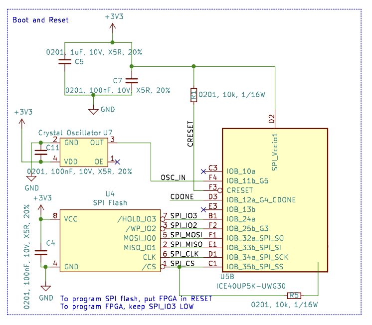
iCE40 components are configured for a specific application by loading a binary configuration bitstream image, generated by the Lattice development system. For high-volume applications, the bitstream image is usually permanently programmed in the on-chip Non-volatile Configuration Memory. However, the bitstream image can also be stored externally in a standard, low-cost commodity SPI serial Flash PROM. The iCE40 component can automatically load the image using the SPI Master Configuration Interface. Similarly, the iCE40 configuration data can be downloaded from an external processor, microcontroller, or DSP using an SPI-like serial interface.
Given that the Fomu is primarily intended for prototyping and education, utilizing the NVCM is unnecessary. However, it does include a GD25Q16CEIGR flash chip for persistent bitstream storage. Despite the Fomu hardware also being open source, I hadn’t spent much time looking at the schematic when developing with it in the past. However, while on the plane ride back from my travels, I was reading some of the documentation for the device and became curious about how the device supported both loading bitstreams into SRAM on the iCE40 and into the external flash.
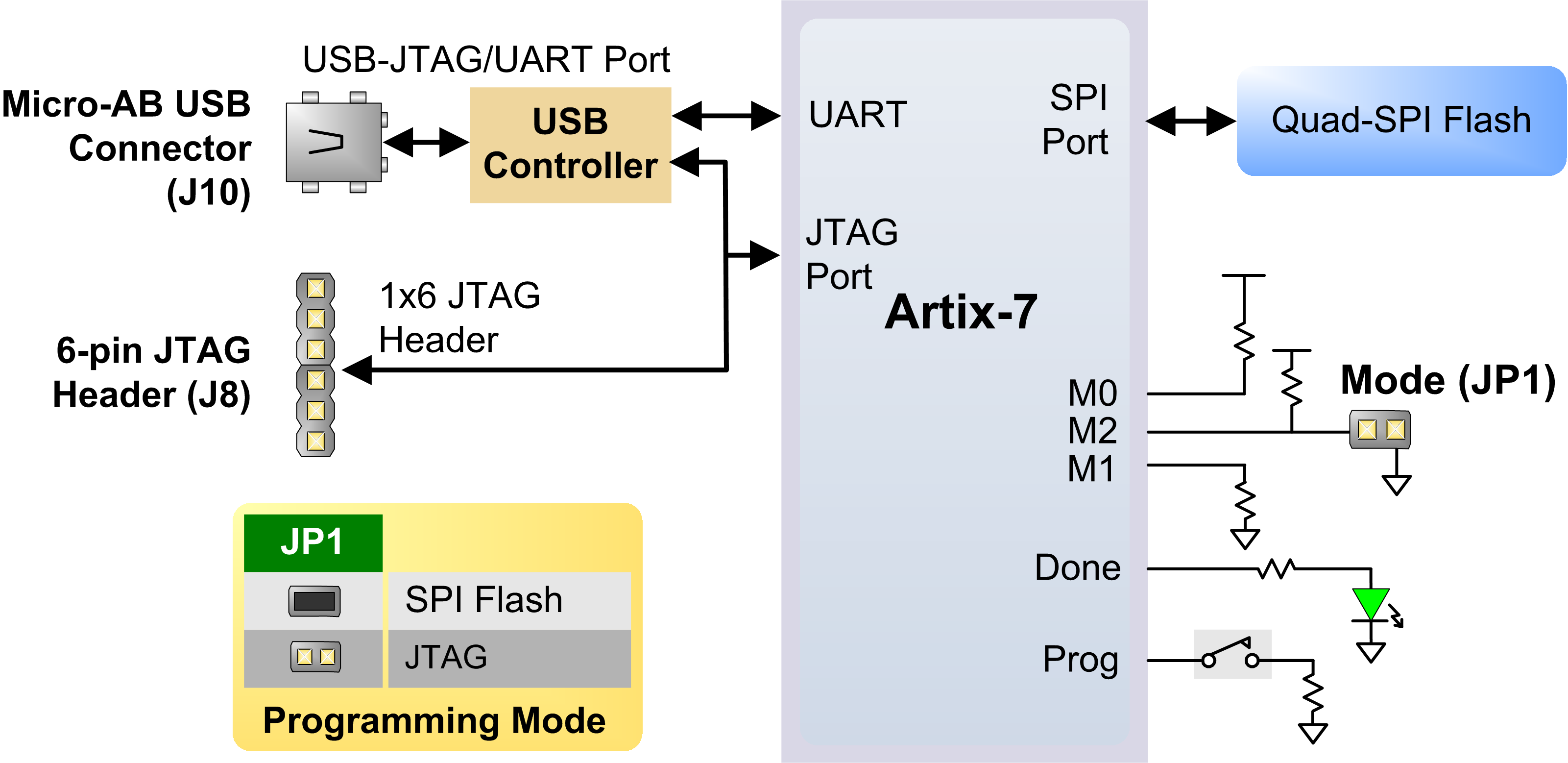
Other FPGA development boards, such as the Arty A7 I have previously written about, support configuring the FPGA’s SRAM by including a USB to Serial IC (the Arty A7 uses the FTDI FT2232HQ) that can be used to configure the FPGA directly, or configure the FPGA with a bitstream that allows it to talk to the SPI flash, which is subsequently used to store the user bitstream in flash. From the Arty A7 reference manual:
When programming a nonvolatile flash device, a bitstream file is transferred to the flash in a two-step process. First, the FPGA is programmed with a circuit that can program flash devices, and then data is transferred to the flash device via the FPGA circuit (this complexity is hidden from the user by the Xilinx tools). This is called indirect programming. After the flash device has been programmed, it can automatically configure the FPGA at a subsequent power-on or reset event as determined by the mode jumper setting.
However, as previously mentioned, the Fomu’s USB core is implemented in RTL, which presents a few challenges. Namely, the FPGA needs to be “bootstrapped” — we cannot configure the FPGA or the SPI flash via USB without the USB core already running on the FPGA. Fomu uses a bootloader, Foboot, which includes gateware for a RISC-V core (VexRiscv) and various peripherals, as well as software for USB and DFU suppport. If you buy a Fomu, Foboot will already be present on the device. You can update Foboot using the Booster program, but if you somehow perform a faulty update, you could find yourself with a bricked device that cannot be accesed over USB. In that case, you’ll need to be able to access the components by some other means. Or, if you’re like me, you might just be interested in loading alternative gateware and software onto the device.
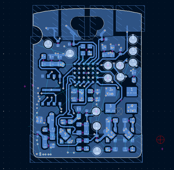
The Fomu hardware repository has a nice image with some of the board’s test points labeled.
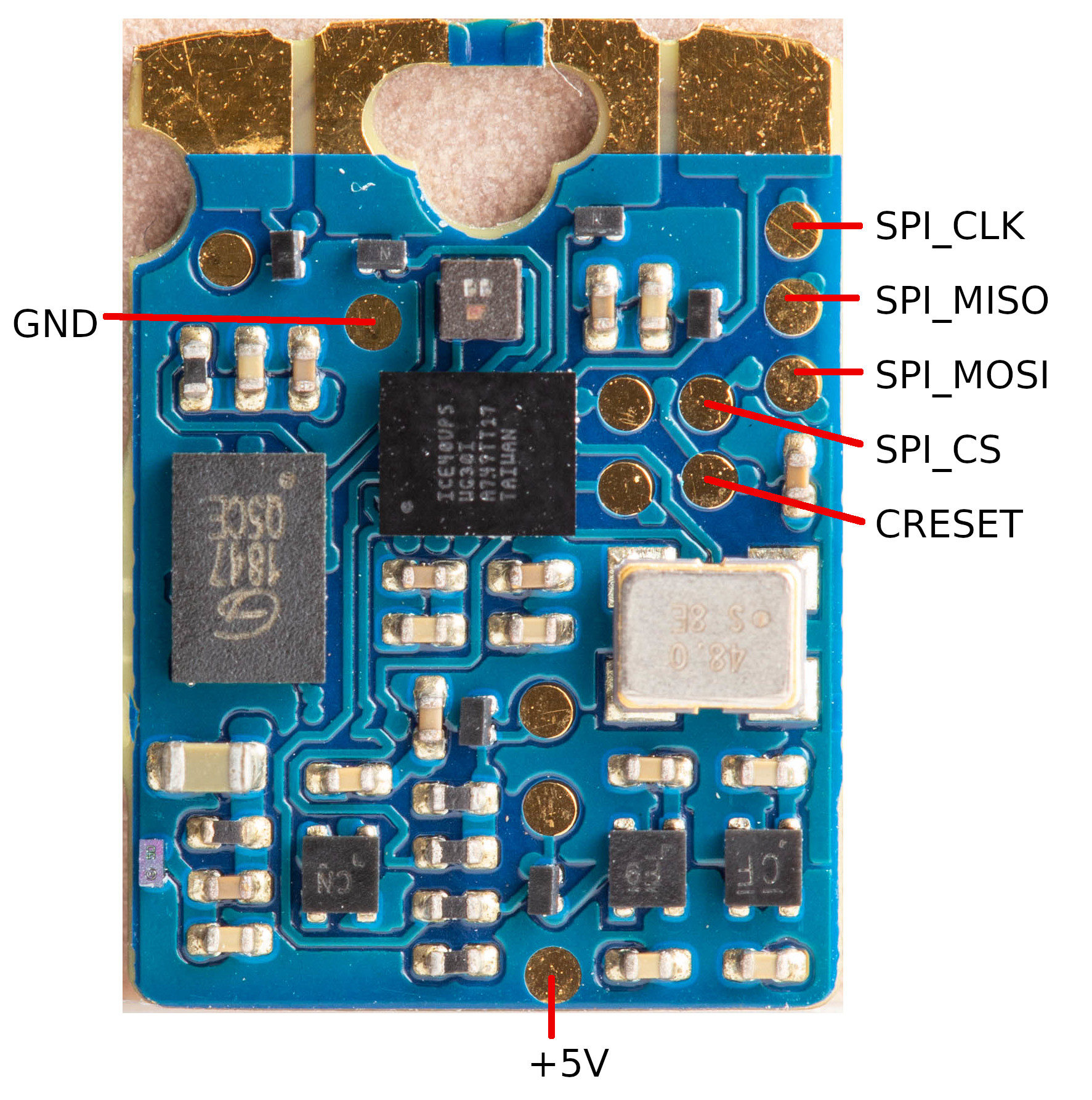
The first thing that I noticed was that there was only one “chip select” (SPI_CS) test point. Both the FPGA and the flash IC can act as SPI peripherals, and typically a CS line is required from the controller to each peripheral in a multidrop configuration, or peripherals can be daisy-chained if supported. The iCE40 is particularly interesting in this scenario because, as previously mentioned, it can act as a controller when reading from the flash IC, or as a peripheral when being configured directly. When supplying power, the iCE40 will act as a SPI controller by default and attempt to load a bistream from the flash IC. If we want to program the flash directly via the test points, then we need to keep the iCE40 from attempting to control it. This is possible because the CRESET pin is also available on a test point.
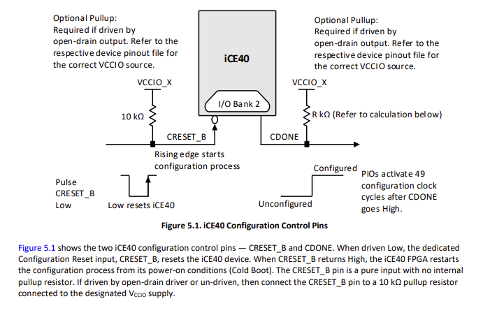
As shown in the technical note, driving CRESET low will reset the device, and configuration will not begin until the next rising edge. At this point it is clear how we can go about programming the flash IC: hold the iCE40 in reset while we program the flash using the exposed SPI test points. One plausible assumption is that only the flash IC can be accessed over SPI via the test points. In fact, we really don’t need direct access to the iCE40 because if the flash IC can be programmed, then the iCE40 will load the persistent bitstream when powered on, and a bricked device could be recovered.
Interestingly, the iCEstick evaluation board made by Lattice Semiconductor, which uses an FTDI FT2232H in similar fashion to the Arty A7, takes this to heart. In the user guide, it states the following under “Known Issue”.
This board is designed for SPI flash programming only. This would prevent the iCE device from being accidentally NVCM programmed.
(This is also called out in the help output for iceprog, a programming tool included in Project IceStorm.)
As you would expect, this is reflected in the schematic from the same document. The SPI chip select pins on the iCE40 and the flash IC have a pull-up resistor, and the iCE_SS_B net allows for pulling the CS pin on the flash IC low for programming, while the iCE40 SPI_SS_B pin drives it after boot when the FPGA is acting as the controller.
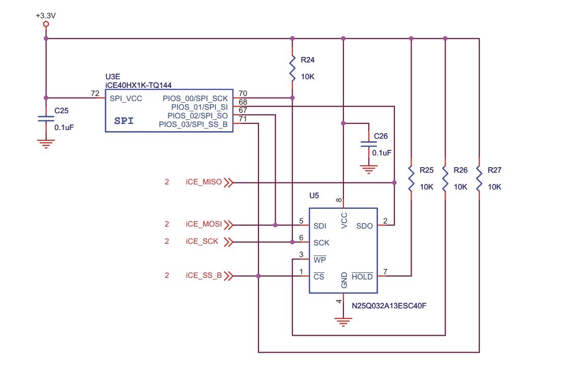
However, as you may have noticed in the first image in this post, the note on the Fomu schematic indicates that both the iCE40 and the flash IC can be programmed via the test points. This complicates things a bit because, up until now, each component only ever plays a single role:
- The iCE40 FPGA is always a SPI controller.
- The programmer (e.g. the machine connected to the test points) is always a SPI controller.
- The flash IC is always a SPI peripheral, either accessed by the programmer or the FPGA.
If we are configuring the iCE40 directly, the iCE40 now needs to act as a peripheral, and the flash IC needs to no longer be driven by traffic on the SPI nets. Though not labeled in the device image, opening the design in the KiCad PCB viewer reveals the placement of the SPI_IO2 and SPI_IO3 (as well as the CDONE, USB_P, and USB_N) test points.
SPI_IO3 is connected to the flash IC HOLD pin. This is in contrast to the iCEstick, where the flash IC’s HOLD pin has a pull-up resistor (i.e. the active low pin is never asserted). Because we have access to the HOLD pin on the Fomu, we can drive it low to have the flash IC ignore all SPI traffic while configuring the iCE40 directly. We also need to swap the pins used for the MOSI and MISO signals, as SPI_MOSI is connected to the iCE40’s SPI_SO pin, and SPI_MISO is connected to SPI_SI. When I looked at fomu-flash, a utility to program Fomu boards using a Raspberry Pi, it appeared as though that was exactly what was happening.
However, upon further inspection, spiHold() is not actually asserting the HOLD pin, but rather issuing a command.
In looking up the spiHold() / spiUnhold() commands in the GD25Q16CEIGR datasheet, I observed that they correspond to “Deep Power-Down (DP)” (0xb9) and “Release from Deep Power-Down and Read Device ID (RDI)” (0xab).
Executing the Deep Power-Down (DP) command is the only way to put the device in the lowest consumption mode (the Deep Power-Down Mode). It can also be used as an extra software protection mechanism, while the device is not in active use, since in this mode, the device ignores all Write, Program and Erase commands… Once the device has entered the Deep Power-Down Mode, all commands are ignored except the Release from Deep Power-Down and Read Device ID (RDI) command. These commands can release the device from this mode.
There are a few reasons why using the power down strategy rather than asserting HOLD may be useful. First, the GD25Q16CEIGR supports Dual and Quad SPI, and in the latter case the HOLD pin is reassigned as the final I/O pin (IO3). If the goal is to configure the iCE40 directly, this may not be too much of a problem, but the Quad Enable (QE) bit is set in a non-volatile status register, so a previous interaction with the device where it was set could cause the HOLD strategy to fail (with the Fomu specifically, I suspect that would also cause issues any time the iCE40 attempted to control the flash IC). Perhaps a more likely motivator is that it reduces the number of test points that need to be accessed to configure the iCE40 directly. Only the 7 labeled in the initial image (5V, GND, CRESET, SPI_MOSI, SPI_MISO, SPI_CLK, SPI_CS) are necessary.
FPGAs are fascinating on many dimensions, but one of the most interesting is how they are configured. As we can see with the Fomu and other iCE40 based platforms, the capabilities of the FGPA can lead to some interesting board desgin decisions.