.png)


There are many reasons why Nvidia is the hardware juggernaut of the AI revolution, and one of them, without question, is the NVLink memory sharing port that started out on its “Pascal” P100 GOU accelerators way back in 2016. And now, after nearly a decade in the field and with the UALink consortium getting ready to gang up on Big Green for memory coherent interconnects for datacenter compute engines, Nvidia has decided to open up access to the NVLink protocol and the physical transports, or PHYs, that drive it.
The resulting intellectual property package is called NVLink Fusion, meaning that those making custom CPUs or accelerators can license the NVLink port designs and the memory atomic protocol that rides on top of it to allow a kind of NUMA memory sharing akin to that which has been available for CPUs for several decades now.
Of course, this technology was always licensable. Every technology is. It is always a matter of haggling about the price. If you cut Intel a big enough check – or sued them in court for antitrust – you could always license the X86 instruction set, just to give an example. As it turns out, it was easier for AMD to sue Intel for the right to use its black box, clone X86 instruction set and then do a cross-licensing agreement with Intel to bury the legal hatchet. Suing Nvidia was not a good option for the industry, but if Nvidia makes a fuss about UALink and its intellectual property, there is no question that the industry will gang up on Nvidia at this point. Everyone agrees – and when we see this, we mean anyone in the IT sector on Planet Earth – that Nvidia needs some competition to drive down prices for AI infrastructure.
It is not Nvidia’s job to do this. Nvidia is supposed to try to get as much revenue and profit during this time, and then squander it stupidly. Like IBM, Microsoft, and Intel have all done in their turn. Buying Arm for $40 billion, as it tried to do back in 2020 through 2022, would have been one such squandering, and Nvidia has probably learned its lesson from that bullet dodge. But had that Arm deal happened, NVLink and its related NVSwitch intellectual property might have already been opened up – and at reasonable prices – for everyone to use through the Arm intellectual property machine, as Nvidia co-founder and chief executive officer Jensen Huang told us from the beginning was the plan.
When the Arm deal did not go through, and Nvidia had to pay Softbank $1.25 billion for killing the deal that antitrust regulators would not support, we reminded Nvidia in early 2022 that what Nvidia couldn’t buy through Arm it could still accomplish through a tighter partnership with Arm or by emulating it with its own IP licensing. Perhaps there have been such talks with the hyperscalers and cloud builders that have decided to go their own ways in designing their own CPUs and AI accelerators and having them fabbed by Taiwan Semiconductor Manufacturing Co. Perhaps not.
There is one CPU maker that has already done such a licensing deal with Nvidia, of course, and that was IBM, which partnered with Nvidia to create the pre-exascale systems combining its Power9 processors and Nvidia’s “Volta” V100 GPU accelerators using the NVLink 2 ports. There was nothing magical going on in this case. IBM had created its own “BlueLink” OpenCAPI PHYs and a NUMA protocol that ran on it to link the Power9 processors to each other in a shared memory NUMA setup. Adding the NVLink protocol to BlueLink this was no big D. And hence IBM was prime contractor for and Nvidia supplied most of the flops for the “Summit” supercomputer at Oak Ridge National Laboratory and the “Sierra” supercomputer at Lawrence Livermore National Laboratory.
But, IBM and Nvidia did not come to terms on how to work together on the exascale systems for these two US Department of Energy labs, and Big Blue did not support NVLink 3.0 ports on the Power10 chips even though we are certain that it was technically possible. (And, probably economically preferable.) So AMD swept in and won those deals and had a chance to vitalize its datacenter GPU business. (You really can’t say “re-vitalize” because it had never amounted to much all of these years. Not so today, though. . . . )
Nvidia’s “Grace” CG100 Arm server processor, of course, has NVLink links on it, and the links are aggregated to bring 600 GB/sec per port of aggregate bandwidth between the CPU and “Hopper” H100 and H200 GPU accelerators or “Blackwell” B100, B200, and B300 GPU accelerators.
NVLink has a variable number of lanes per link, two lanes per link for bi-directional traffic, and multiple links to create a physical port running, and the lanes run various speeds depending on the generation and the use of PAM-4 modulation on the signals. Like this:
- NVLink 1.0 had lanes that ran at 20 Gb/sec and eight lanes per link with 40 GB/sec of bi-directional bandwidth per link. With four links per Pascal P100 accelerator, Nvidia delivered 160 GB/sec of bandwidth between the GPUs and to the Power8 CPU that had experimental NVLink 1.0 ports.
- With NVlink 2.0, the lanes ran at 25 Gb/sec (the same as IBM’s BlueLink), and there were eight lanes per link again, which yielded 50 GB/sec of bi-directional bandwidth per link. The V100 GPU had six links aggregated, delivering 300 GB/sec of bandwidth between devices.
- With NVLink 3.0, PAM-4 modulation was added to the NVlink SerDes, doubling the lane bandwidth, but the number of lanes per link was halved to four, which kept the bi-directional bandwidth per link at 50 GB/sec. The “Ampere” A100 GPU had a dozen NVLink 3.0 ports, which yielded 600 GB/sec of bandwidth. (This is what the Grace CPU has as well.)
- With NVLink 4, the signaling rate is boosted to 100 Gb/sec (50 Gb/sec native with PAM-4 encoding added), and there are two lanes per link for the same 50 GB/sec bi-directional signaling rate per link. The Hopper and Blackwell chips each have 18 links per chip or, in the case of Blackwell, chiplet, and that yields the 900 GB/sec of bi-directional bandwidth per Hopper or Blackwell GPU chiplet. (The Blackwell socket has two chiplets, and gets 1.8 TB/sec of NVLink 4.0 bandwidth.)
- As we explained back in April, UALink can gang up more lanes and as many links to dial up the bandwidth into and out of accelerators and CPUs. UALink will run lanes at 200 Gb/sec (100 Gb/sec native signaling plus PAM-4 encoding) with four lanes for a 800 Gb/sec link, which is 1,600 Gb/sec bi-directional per link. Gang up four of these links, and you can create a UALink port that runs at 800 GB/sec, which is probably close enough to the 900 GB/sec per port that NVLink 4 is delivering for Hopper and Blackwell.
With NVLink Fusion, Nvidia is not opening up NVLink and NVSwitch, and it most definitely not creating a free-for-all (in either senses of those words) that will let anyone making a CPU or an accelerator graft NVLink memory atomics to their devices.
There are two approved uses cases for NVLink Fusion.
The first is to add NVLink ports to a custom CPU, such as the ones that the hyperscalers and cloud builders are designing for their own use. This assumes that those hyperscalers and cloud builders will use NVLink to hook Nvidia GPU accelerators to those homegrown accelerators. In the diagram that we have seen, the hardware stack includes Spectrum-X switching and BlueField or ConnectX network interface cards hooking into the CPU for the east-west and north-south networks, with Nvidia GPUs cross-coupled with NVSwitch and using Nvidia’s Mission Control system control software. It is not clear if all of these components are required to be able to add NVLink to the custom CPU silicon.
The other use case is to use Nvidia’s current Grace CG100 Arm processor or the future “Vera” CV100 CPU from Nvidia and an NVLink C2C die-to-die interconnect to link to a custom accelerator that has NVLink Fusion ports on it. The same front end Spectrum-X and BlueField/Connect-X network and the same NVSwitch and Mission Control back end network are wrapped around it. Again, it is not clear if this is required to be able to add NVLink ports to custom accelerators.
There are no scenarios where you can use NVLink ports on custom CPUs and custom accelerators with NVSwitch interconnects or directly linked like superchips or in all-to-all configurations with two, four, or eight accelerators. Just those two options discussed above.
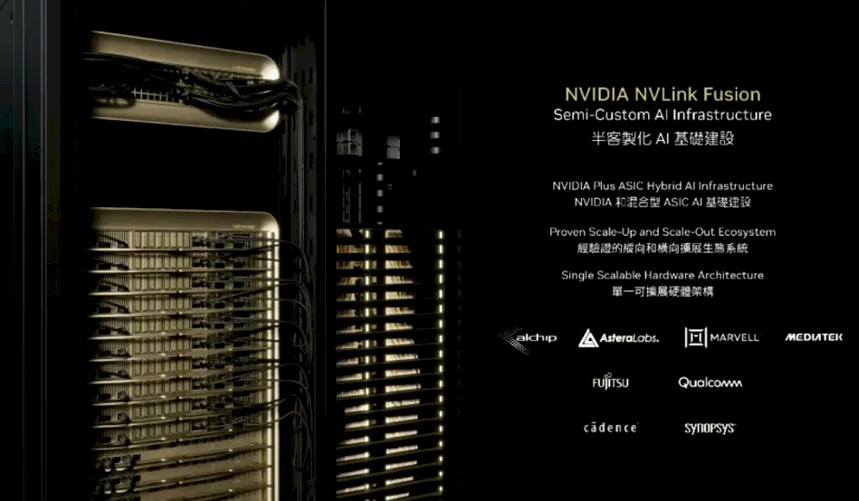
Nvidia has both Cadence Design Systems and Synopsis as technology partners to help customers design NVLink ports into their CPUs or accelerators. Alchip, Astera Labs, Marvell, and MediaTek are all able to do the custom design work to add NVLink Fusion ports to devices, and Fujitsu and Qualcomm have signed up to add NVLink Fusion ports to their datacenter CPU designs. Qualcomm also has AI accelerator aspirations and may be adding NVLink to those devices, too, but they will have to link to Nvidia Grace or Vera CPUs to do it, apparently.

Sign up to our Newsletter
Featuring highlights, analysis, and stories from the week directly from us to your inbox with nothing in between.
Subscribe now