.png)

This is part 2 of my ongoing series about LATENTRED, my project to create an open source 1U managed Ethernet switch from scratch.
Today, we’re going to be talking about the 24-port QSGMII line card. Two of these will provide all of the front panel connectivity for the edge-facing side of the switch (i.e. everything but uplink and management ports).
Overview
Here’s the line card before heatsink installation. This is “upside down” in the canonical CAD layout, but provides a better view of the layout without the RJ45s blocking the view.
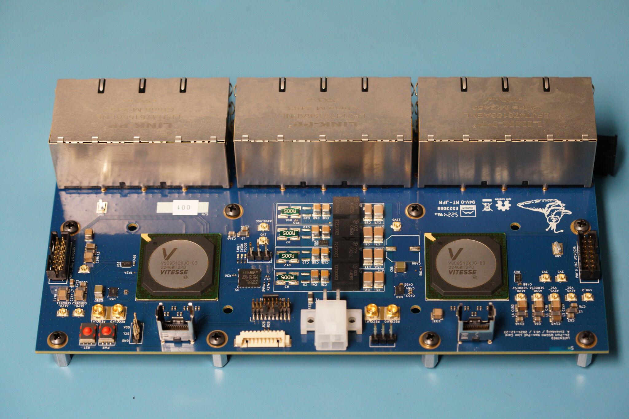
The overall layout of the board is mostly symmetric, but with some variations because of the PHYs not being mirror images of each other.
At the north side we have the three 8-port RJ45s. These are Link-PP LPJT476156AENL and among the most expensive parts on the board at $33 each (plus tariff for any I need beyond the initial ten samples I got for prototyping), second only to the $40.11 PHYs.
Speaking of PHYs, the two large BGAs are Microchip (formerly Microsemi, formerly Vitesse - yay semiconductor industry M&A) VSC8512 12-port QSGMII PHYs. Each PHY is responsible for half of the front panel ports on the line card (one quarter of the whole switch).
These are older 65nm parts, but as of when I last checked they were the only 12-port QSGMII PHY available from distributors in low volume with a datasheet that isn’t NDA-encumbered, so I’m stuck using them. One of their quirks is that the low speed digital GPIOs (MDIO, reset, JTAG, etc) are LVCMOS25 rather than the LVCMOS33 or LVCMOS18 in more common use in modern parts. This doesn’t change a whole lot on the line card board, but does cause some annoyances on the switch engine board which we’ll discuss in a future post. Each PHY has a probably-unnecessary JTAG connector, using the 2x7 Xilinx pinout since I have a lot of those dongles, in case I want to do boundary scan test. So far I haven’t needed this.
On the far east/west sides of the board next to the JTAG connectors are a series of power rail test points (more on that in a bit) and filtering components for the various isolated analog domains on each PHY. This area also contains an AT30TS74 I2C temperature sensor to measure board temperature in the general area of the PHY.
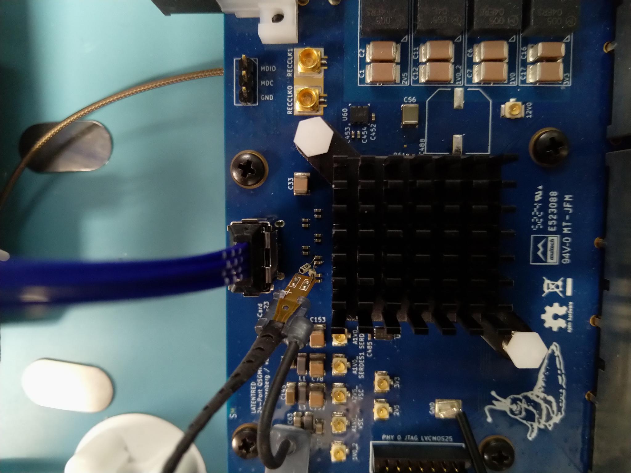
Directly to the south of each PHY is a Samtec ARF6 series connector. This carries eight 100Ω differential pairs, although only six are used here (three TX and three RX lanes). Using this “flyover” architecture allows the PCB to be made of an inexpensive material (Shengyi S1000-2M, relatively standard high-Tg FR-4) without the 5 Gbps signals suffering significant losses from long distance routing on a high-Df material. These links are AC coupled on the line card for both TX and RX. Slightly to the west of each is a pair of SMPM connectors which can be configured to output a recovered clock if I ever need this for validation/test purposes.
In the far southwest corner are power and reset buttons for debug. These drive GPIOs on the supervisor MCU and aren’t intended to be used in the final system, which will allow the line card to be remotely managed over an I2C or SPI bus from the FPGA or main processor.
Just west of the centerline along the south edge of the board is a ten-pin Molex PicoBlade connector which carries all of the low-speed management traffic: I2C to the MCU and sensors, SPI if I want more bandwidth to the MCU, and the MDIO bus for configuring the PHYs.
Down the centerline, we have the power supply - four Murata MYMGK00504ERSR 4A DC-DC modules. These are all fed by a common 12V input on the 4-pin Molex Mini-Fit Jr connector at the south center edge of the board, and each drives one of the board’s four core power rails: 3.3V, 2.5V, 1.0V digital, and 1.0V analog. This area also has another AT30TS74 to monitor PSU temperature, and an INA230 shunt monitor on each rail to monitor current and voltage.
Finally, sandwiched between the PSU and the PHY to its west, is the supervisor. This is a STM32L431 that controls enables and sequencing for all of the power rails, reset and power-down control for the PHYs, and monitors for fault conditions such as a power rail dropping out of regulation or a temperature limit being hit.
Power
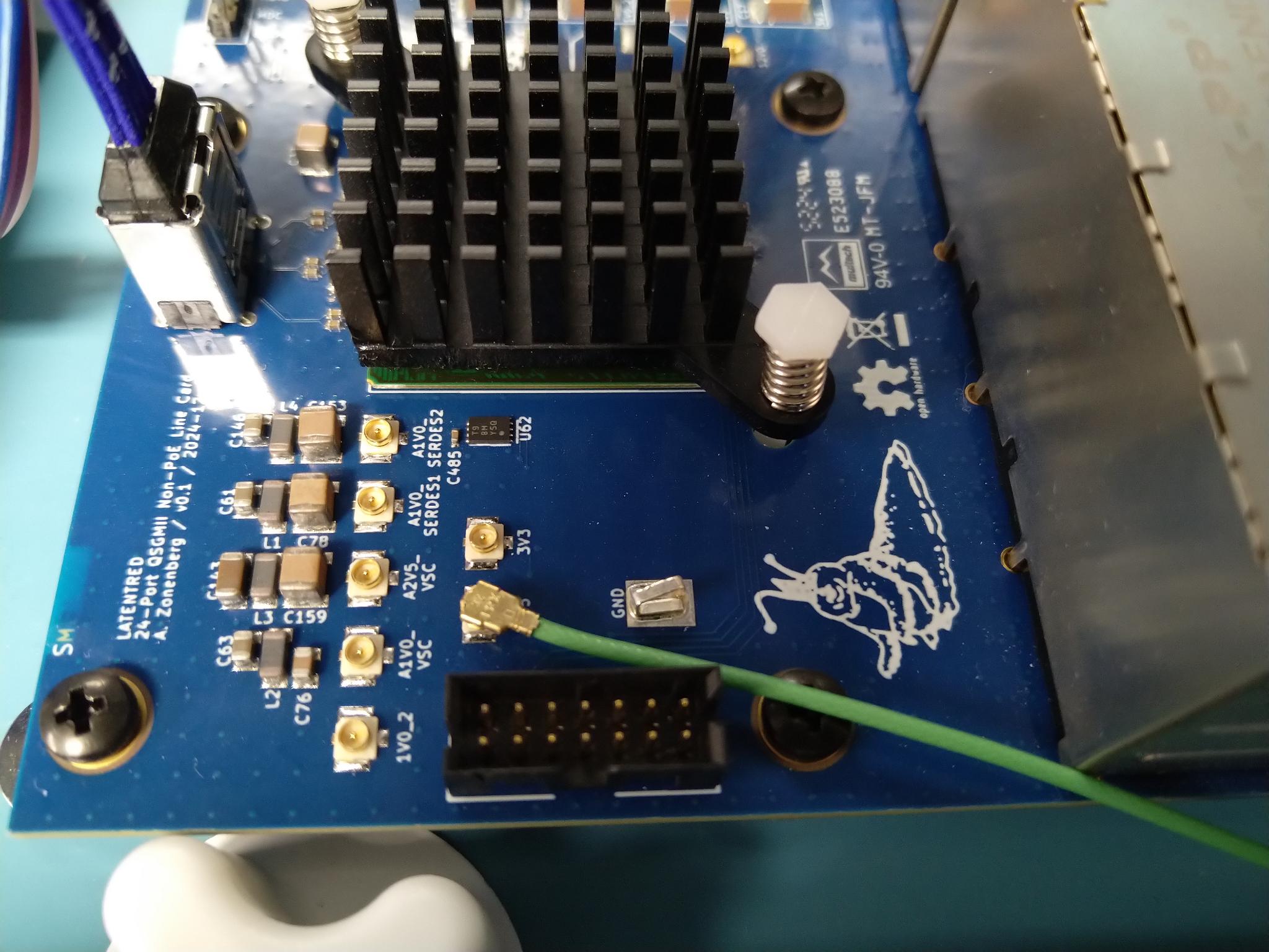
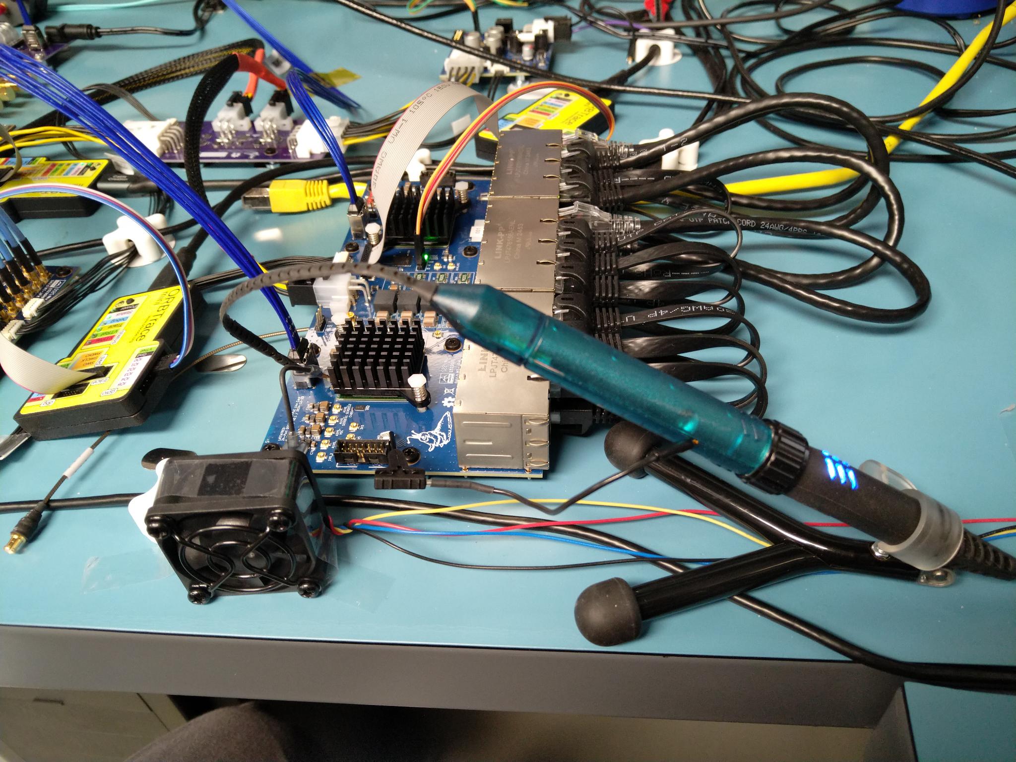
I did initial power supply validation on the line card sitting at idle with 23 of 24 ports linked up, 22 through a set of 11 loopback cables and the 23rd cabled to the sandbox VLAN on my lab network. There’s no traffic flowing other than normal ambient network broadcasts on port 0 because I haven’t finished the gateware enough to actually be passing packets, but this is the best I can do at the moment.
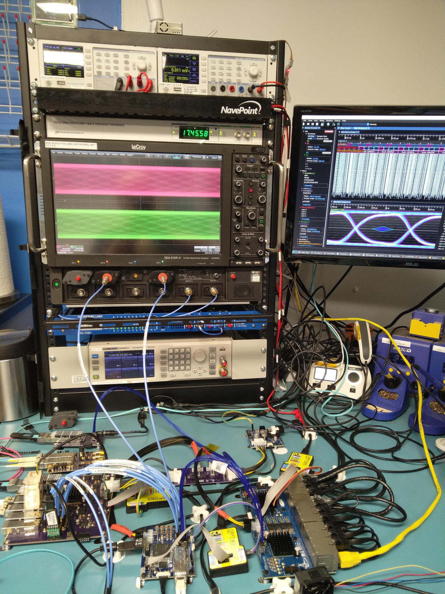
Voltage and ripple measurements were taken with a Teledyne LeCroy WaveRunner 8404M-MS oscilloscope and RP4030 active power rail probe. Current measurements used the shunt resistors and INA230s integrated into the on-board PSU.
3.3V
This rail feeds the supervisor, I2C sensors, and the high side of the port status indicator LEDs. It’s always on, since the line card doesn’t have 3V3_SB routed to it and I didn’t see the point in adding a fifth regulator since it has no sequencing requirements relative to the other rails.
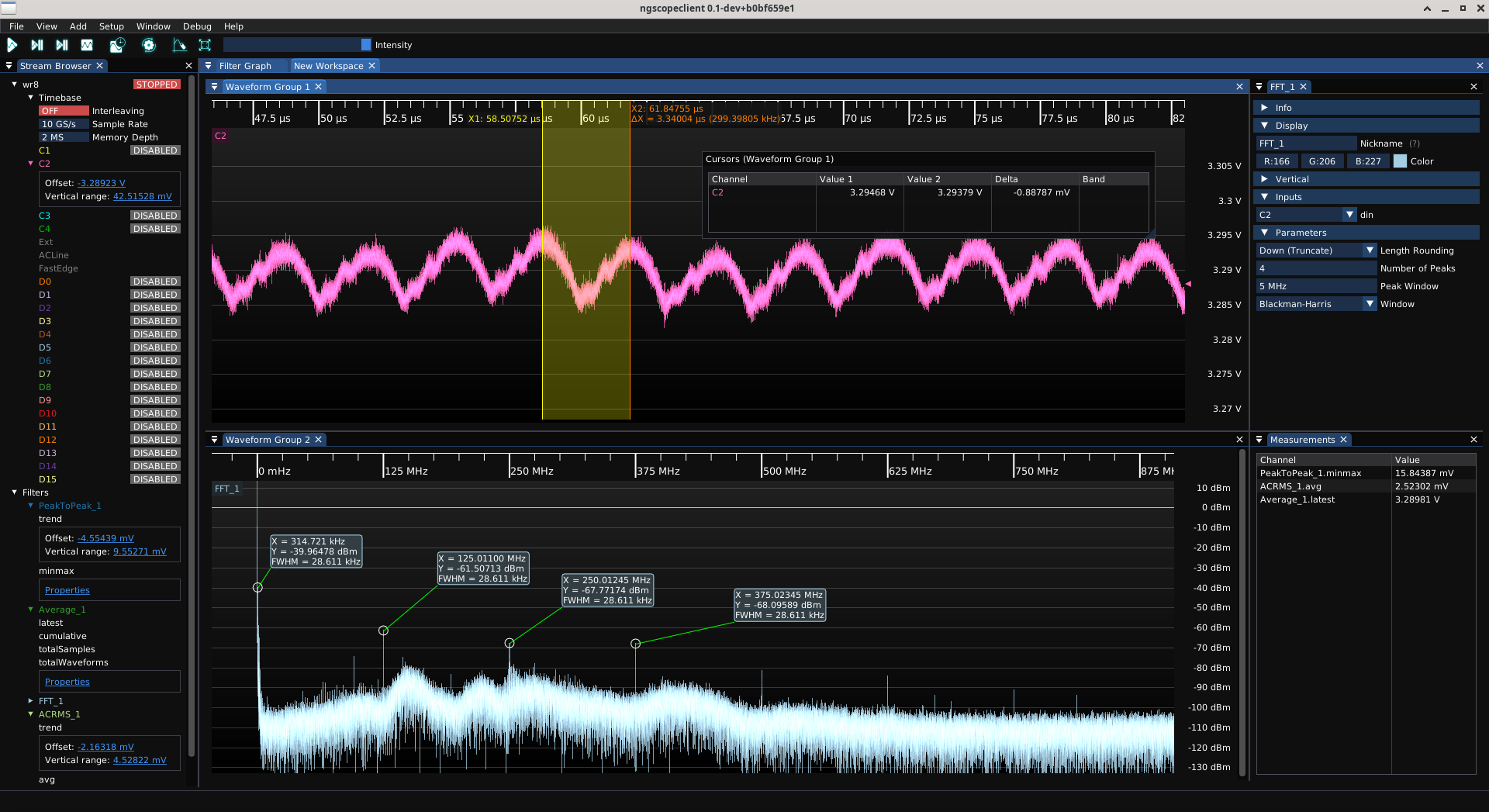
Voltage is 11 mV, or 0.3%, below nominal. Considering I used 1% resistors on the feedback network, I’m happy with that.
Current consumption is around 174 mA at 3.289V, for a total of 572 mW.
I think a sizeable amount of this is in the port indicator LEDs (which are rated for 20 mA each although I’m driving them slightly less hard than that). I’m not sure why RJ45s always seem to be using the old yellow-green AlGaP LEDs rather than the modern emerald-green InGaN ones, I could probably cut almost a watt off my system power budget if I were able to switch, but it was hard enoguh to find high-density jacks with integrated magnetics and AC coupled center taps for voltage mode PHYs.
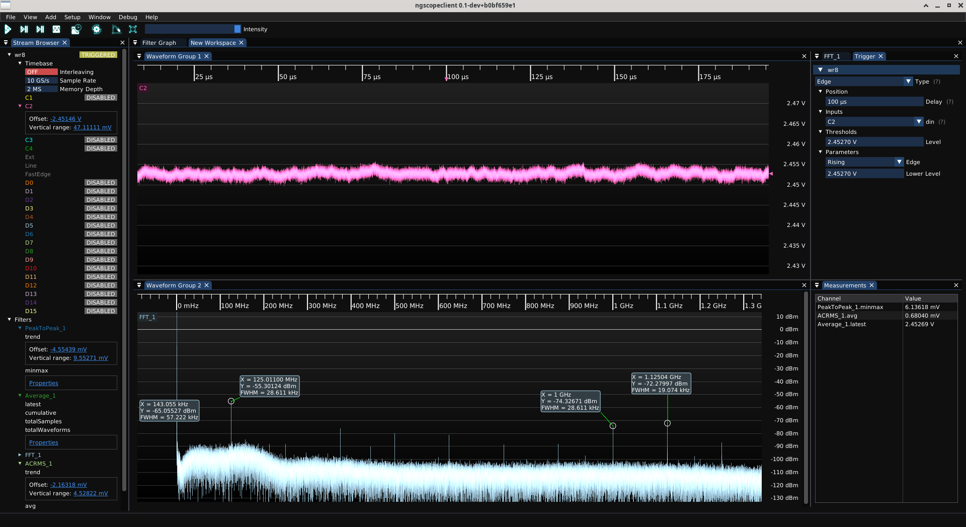
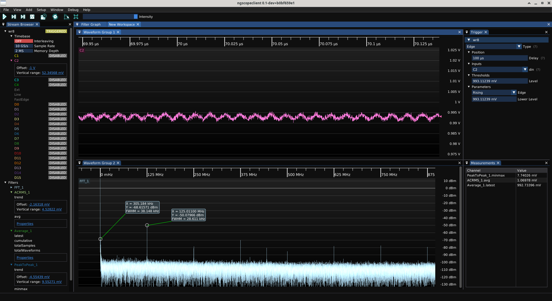
Ripple is very good, 15.8 mV P-P and 2.52 mV RMS. It’s dominated by 300 kHz switching ripple with high frequency noise at 125 MHz and harmonics thereof (obviously coming from the PHYs, maybe the LED drive circuitry or something). There’s also a 95 MHz spectral line I can’t readily explain. I thought it was the supervisor MCU core clock at first, but that’s running at 80 MHz so as soon as I dropped a cursor on the peak I discarded that hypothesis… but it’s at like -75 dBm so I don’t particularly care. It’s not remotely strong enough to be a problem.
2.5V
This is by far the biggest power hog on the board, driving both the LVCMOS GPIO pads on the PHYs (for MDIO and LED drive) directly, and (through a pi filter network) the analog PAM-5 drivers for the twisted pair.
Main rail
Voltage is 21 mV, or 0.84%, below nominal, Also well within acceptable limits.
Ripple is excellent, 6.9 mV p-p and 788 μV RMS. Interestingly it’s not just sinusoidal ripple, there’s a noticeable switching spike right around the zero crossing of the ripple waveform. It’s tiny, maybe a millivolt or two, but clearly visible. (Have I sung the praises of the RP4030 enough? I love it enough that when I saw a second one for a good price, I couldn’t resist jumping on it)
A2V5_VSC
This rail is the analog supply for the PAM-5 twisted pair drivers.
Voltage is sagging well below nominal at 2.452V (48 mV low) due to significant losses in the filter network, but with 70 mV of headroom above the 2.38V lower limit in the datasheet and almost no ripple, so I see no reason to change the design.
Ripple is very close to that on the main rail, 6.13 mV p-p and 680 μV RMS. Perhaps in future designs I can omit this filter entirely unless I have major noise sources on the 2V5 rail that might cause problems? Not worth a board spin when I already have enough bare boards to finish the project, though.
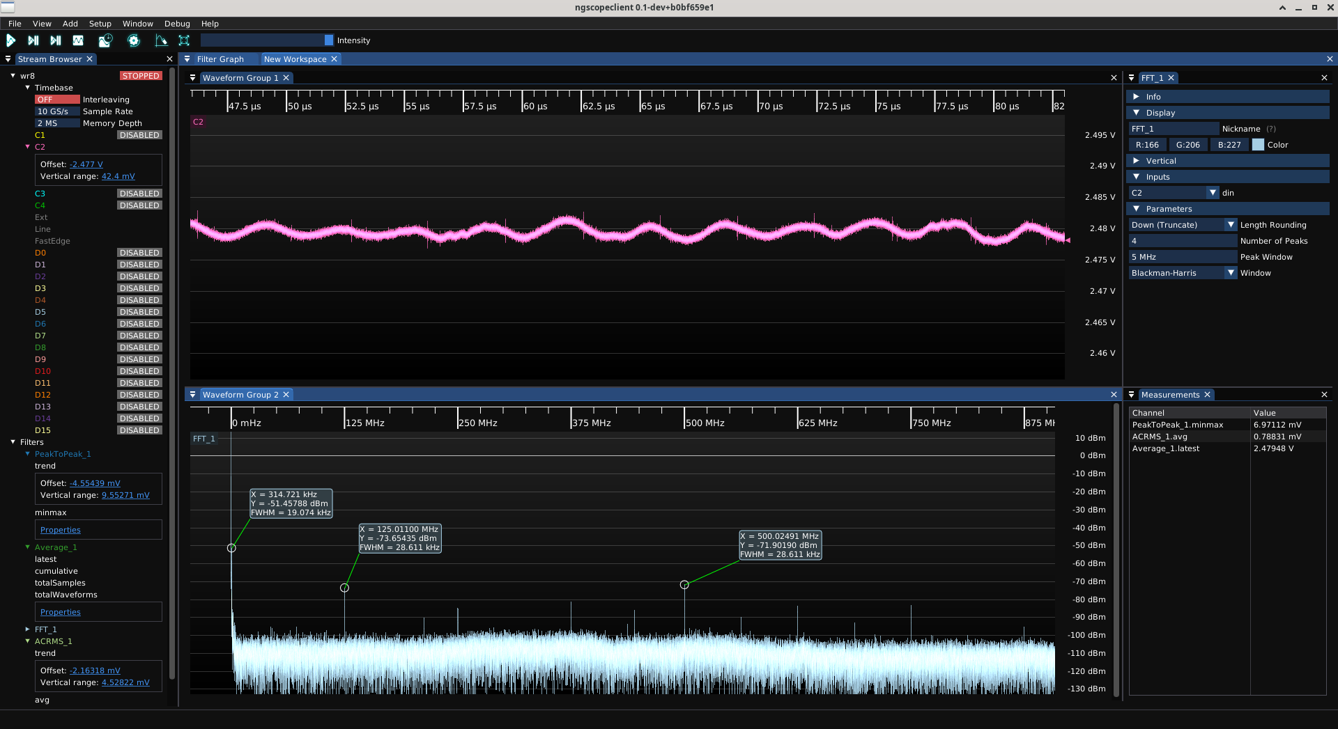
1.0V digital
The 1V0 rail is the second most heavily loaded, driving the digital core of both PHYs. It’s a near perfect 1.000V on average, drawing 2.03A - almost as much current as 2V5, but far less power due to the lower voltage.
Ripple at first glance was… not great, not terrible: only 1.77 mV RMS but 42 mV p-p with strong spikes at the 300 kHz switching frequency.
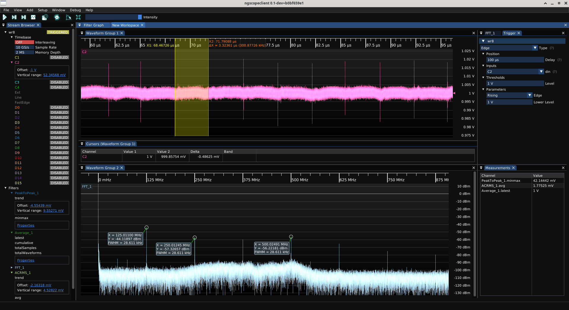
Zooming in, we can see the main high frequency noise on the rail is a somewhat triangular looking 125 MHz about 5 mV p-p,
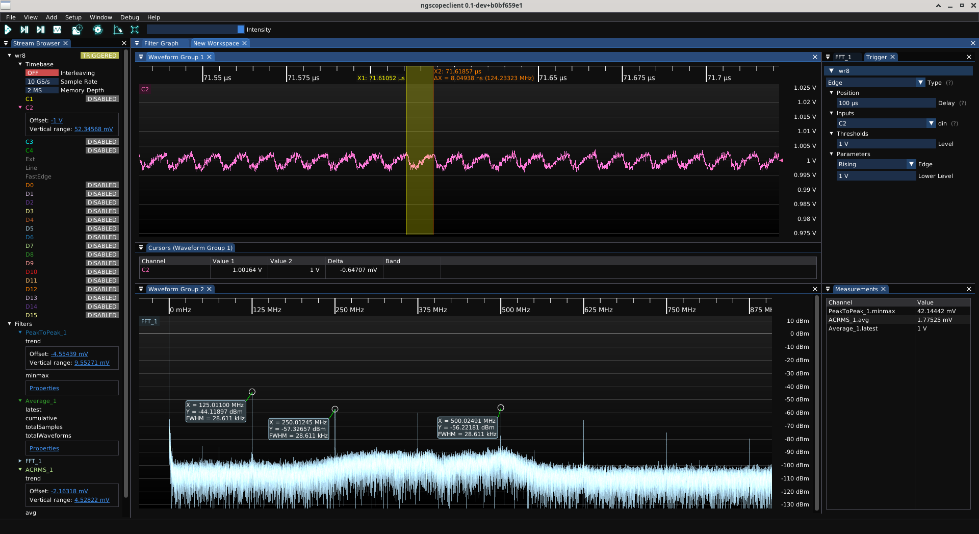
After some investigation, though, the spikes turned out to be a measurement artifact - the test point was placed right next to the DC-DC converter and did not accurately account for the filtering effect of the 40+ high frequency decoupling capacitors under the PHY itself. All of the other rail test points were much closer to the PHYs which gave the capacitors time to do their job.
Measuring with a soldered probe directly under the PHY, we see a drop of about 7 mV in the PDN, but ripple is much lower: 1.06 mV RMS and 7.7 mV p-p with no strong switching spikes visible at all. So the rail is totally fine where it counts, we just need to be measuring at the right spot.
1.0V analog
The 1V0_2 rail is the third most heavily loaded, drawing about 820 mA, and is also almost exactly at the nominal voltage of 1.000V.
Main rail
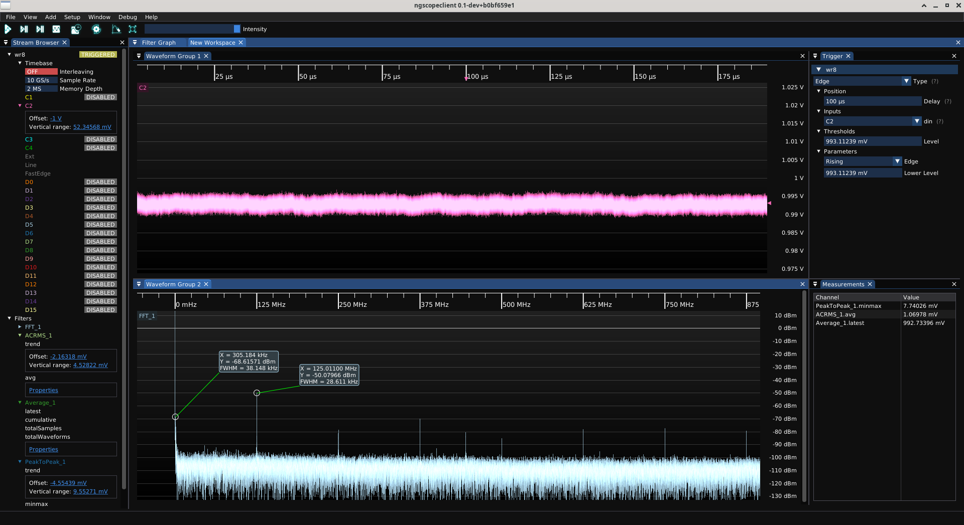
This rail does not directly drive any loads (it feeds six separate analog power domains, three per PHY, through pi filters) so unsurprisingly it’s extremely clean: 5.46 mV p-p and 487 μV RMS. The strongest spectral line is 625 MHz, the 5th harmonic of the 125 MHz main clock frequency.
A1V0_VSC
This is the VDD_AL rail on the left PHY (right is nearly identical), which powers analog circuitry for the twisted pair interface. There’s no current shunt so I don’t know how much of the total 1V0_2 current is consumed by this power domain.
Voltage is slightly lower than nominal (due to losses in the pi filter) at around 996 mV, but well within acceptable limits.
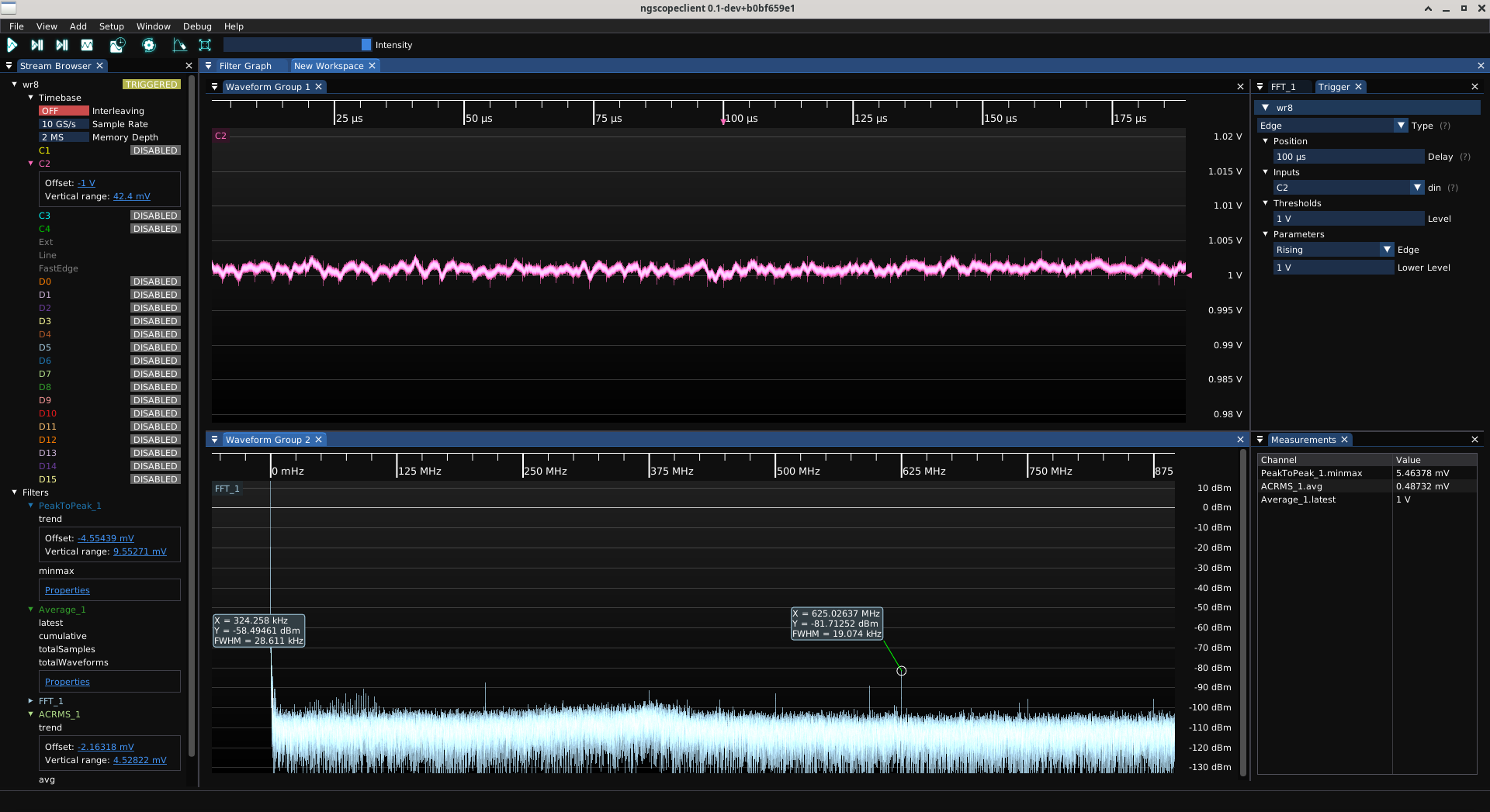
Ripple is excellent, 6.27 mV p-p and 785 μV RMS. 125 MHz and 500 MHz are the dominant spectral lines and the 300 kHz SMPS frequency is almost completely invisible.
A1V0_SERDES1
This is the VDD_A rail on the left PHY, which powers one of two analog domains for the QSGMII SERDES.
As with the other analog rails the voltage is slightly lower than nominal due to filter losses, at 996 mV, but not to a concerning level.
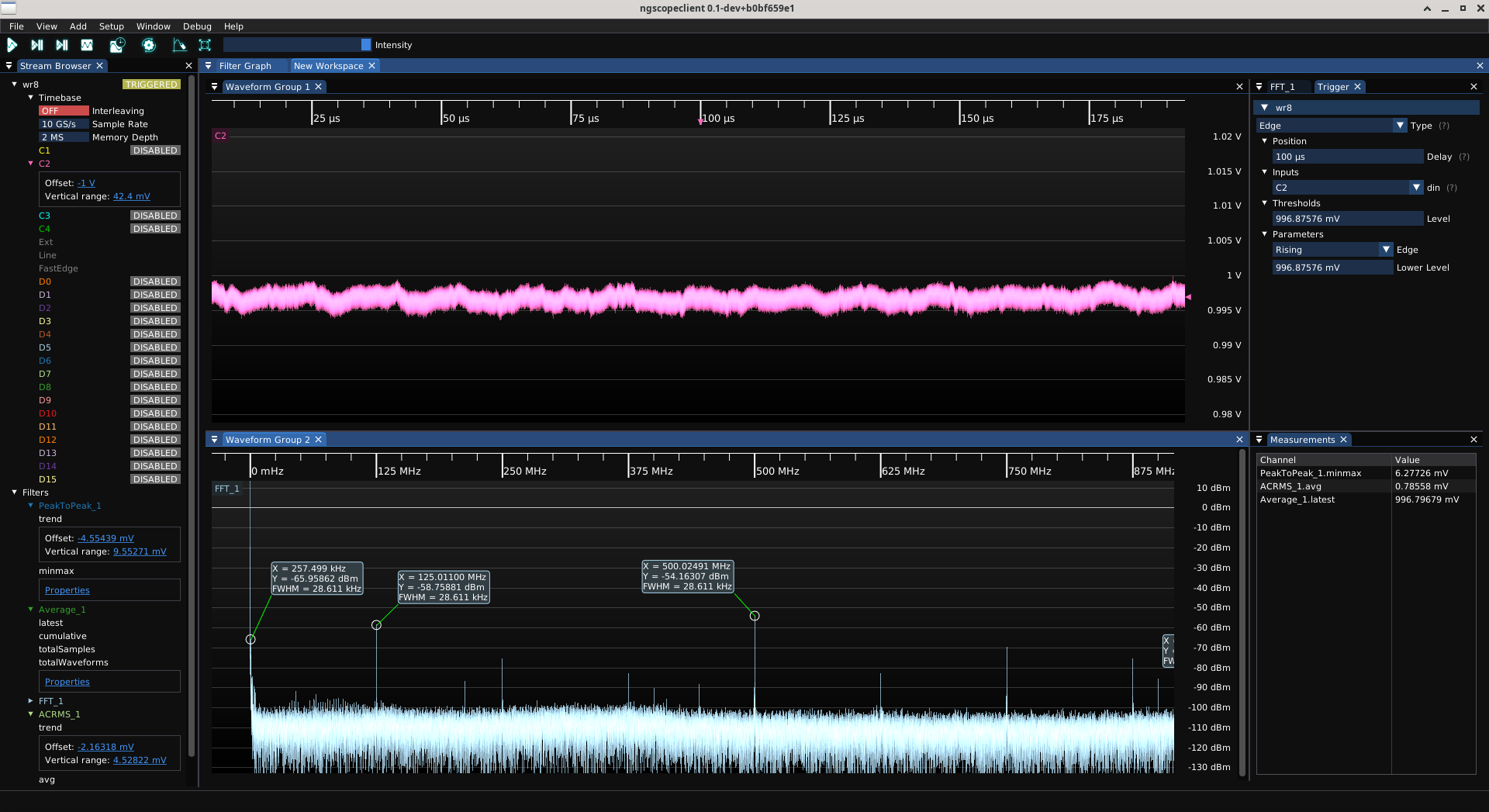
Ripple is extremely low, at 3.85 mV p-p and 438 μV RMS - exactly what we want for something powering a sensitive SERDES. 125 and 625 MHz are the dominant lines, with a noticeable 1 GHz component as well.
A1V0_SERDES2
This is the VDD_VS rail on the left PHY, which powers the second analog QSGMII SERDES domain. Voltage is about 1 mV lower than nominal due to filter losses.
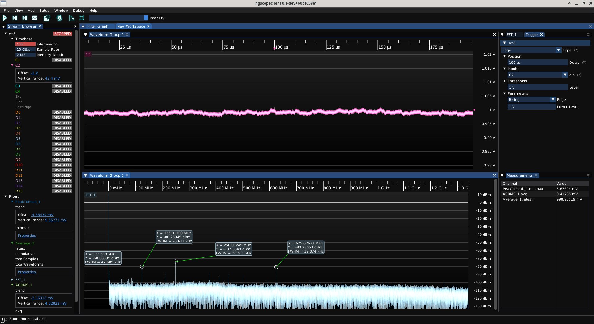
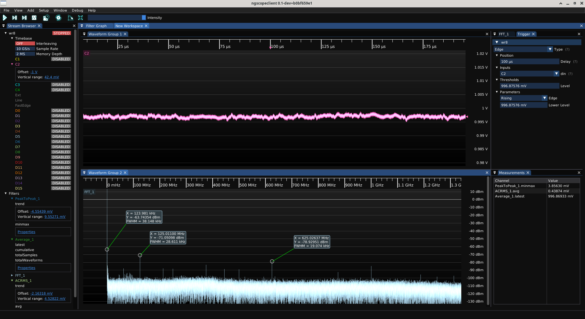
Ripple is the lowest of any power domain on the board, at 3.67 mV p-p and 417 μV RMS. I think this might actually be a personal record for the cleanest SMPS-derived power rail I’ve ever measured on one of my boards. Just to be clear, this is not a 20 MHz band-limited measurement. This is measuring from a few kHz out to 4 GHz using the full bandwidth of the scope and RP4030!
QSGMII
The line card communicates to the host FPGA via six QSGMII links, three per PHY. These are 5 Gbps NRZ and the highest speed signals on the board by far, so I kept the path lengths very short to avoid losses in the cheap Shengyi S1000-2 PCB material, allowing me to keep costs down vs a more expensive low-loss dielectric.
TX
I measured the TX waveform at the AC coupling caps (about 5mm of PCB trace away from the BGA balls and as close as I could practically get) with a 13 GHz LeCroy D1330 active differential probe.
In the test setup, I’m driving the QSGMII with a GTYE4 transceiver on the XCKU5P FPGA through 51mm of trace on Isola FR408HR, a SMPM connector, 12 inches of Koaxis KF086, another SMPM, 46 mm of trace on Shengyi S1000-2, an ARF6 connector, 12 inches of Samtec ARC6 cable, an ARF6 connector, and a few mm of trace on S1000-2.
The real-world deployment will be similar overall trace lengths, but the FPGA board will be Taiwan Union TU872SLK (similar Df to FR408HR) and the SMPM connectors will not be present - there will be a direct 1-2 foot ARC6 connection from the FPGA board to the line card. So in terms of overall insertion loss this is a pretty representative worst-case channel of what we’d see in the real switch.
With the somewhat arbitrarily chosen default TX equalizer coefficients, the eye is open but some closure from losses is clearly visible.
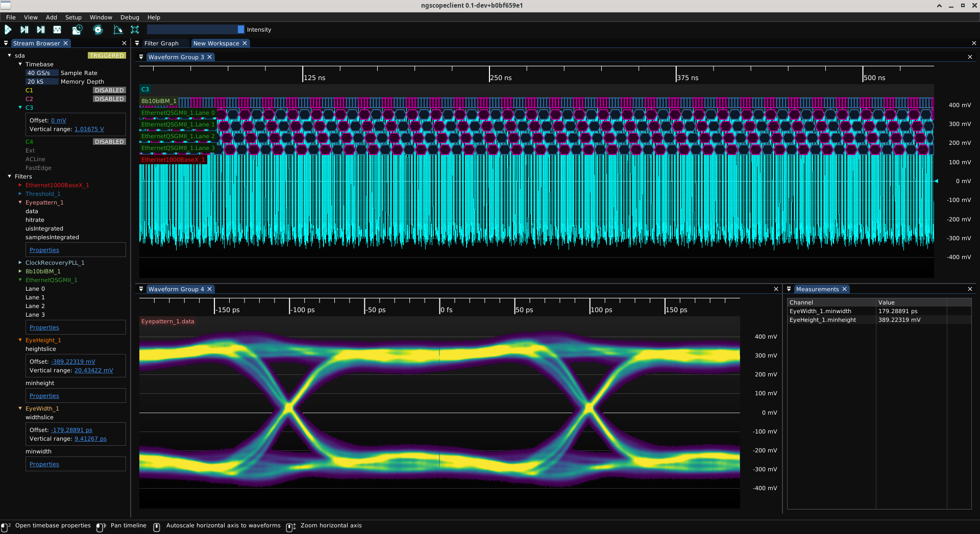
After a bit of tinkering with tap values I settled on TXDIFFCTRL=5’h13, TXPOSTCURSOR=5’h07, TXPRECURSOR=5’h04 which gave a wide-open eye with 179 ps (of the 200 ps UI) of horizontal opening and 389 mV of vertical. This easily passes the QSGMII RX eye mask. I’ll need to tune these values slightly in the final switch deployment for absolute best SI due to the different cable lengths, but this should get me pretty close and is honestly probably not worth changing at this point.
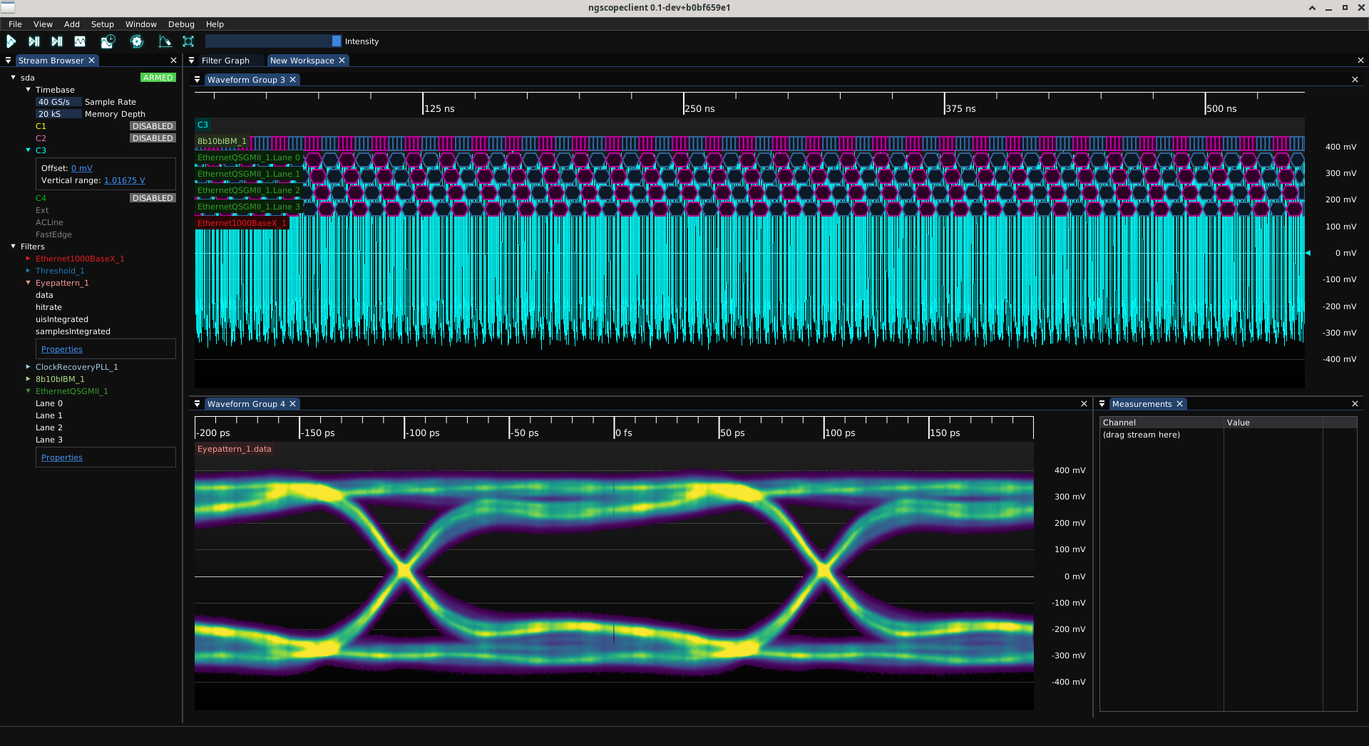
RX
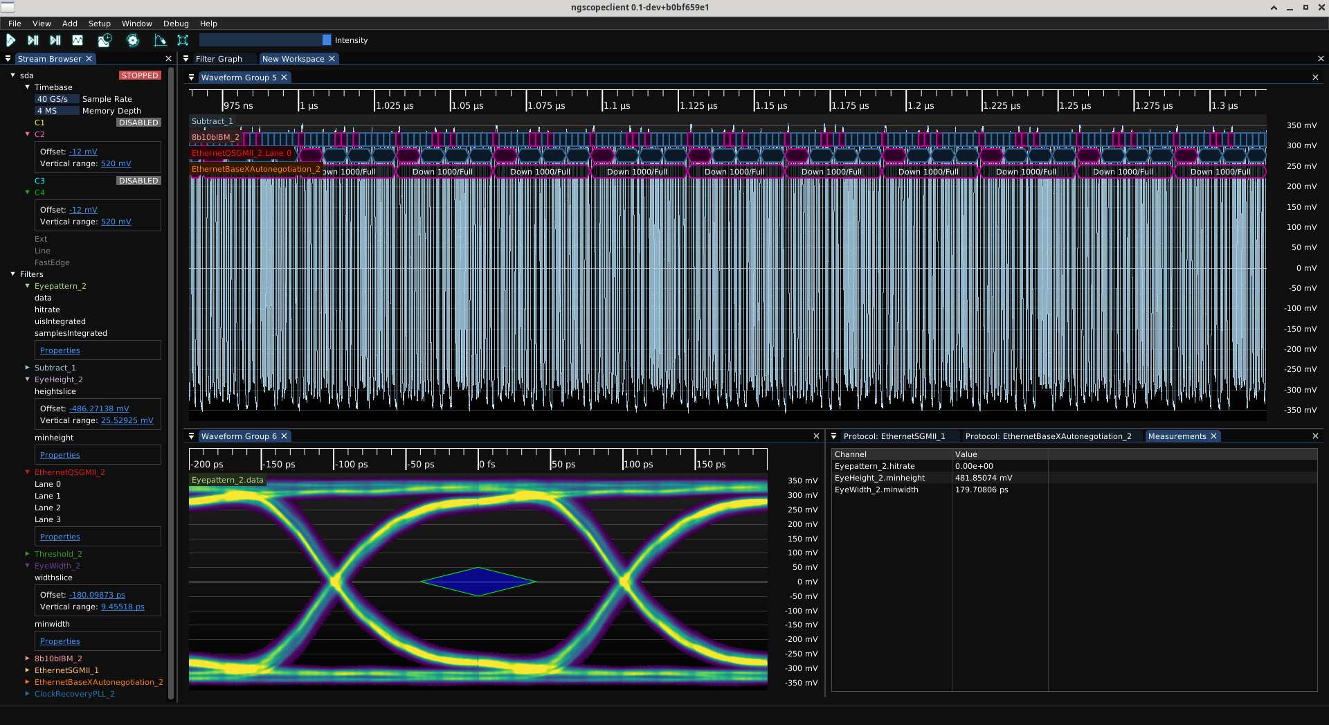
I measured the RX waveforms at the ARC6-to-SMPM adapter board on my bench setup, directly connecting to the oscilloscope through coaxial cabling. The total channel length here is 24 inches of Koaxis KF086 and 12 inches of Samtec ARC6 plus roughly 50mm of PCB trace on S1000-2M (40mm on the adapter board, 10mm on the actual line card).
I deliberately didn’t de-embed the KF086 test leads (even though they are serialized and I have touchstone files for them) since some of the final switch paths may use more than 12 inches of ARC6, so I wanted a bit of extra loss to give a worst-case scenario.
The eye was wide open (481 mV height, 179 ps opening) and passed the QSGMII eye mask with room to spare, but definitely could do with a little bit of emphasis to be perfect (and the swing was actually on the high side, I could probably reduce it to save power). Unfortunately the VSC8512 datasheet does not document the SERDES output buffer configuration registers. I opened a support case with Microchip and if I hear back about this will attempt to tune further, but if not this is absolutely usable as-is.
It’s interesting to compare the rise time and overall eye shape of the RX path (Vitesse 65nm SERDES6G macro) to the TX path (Xilinx 16nm GTYE4 macro). The RX is a 6 Gbps SERDES working at close to its max rated data rate - although still giving a very clean eye - while the TX is a 28 Gbps SERDES that’s not even breaking a sweat and clearly has plenty of headroom.
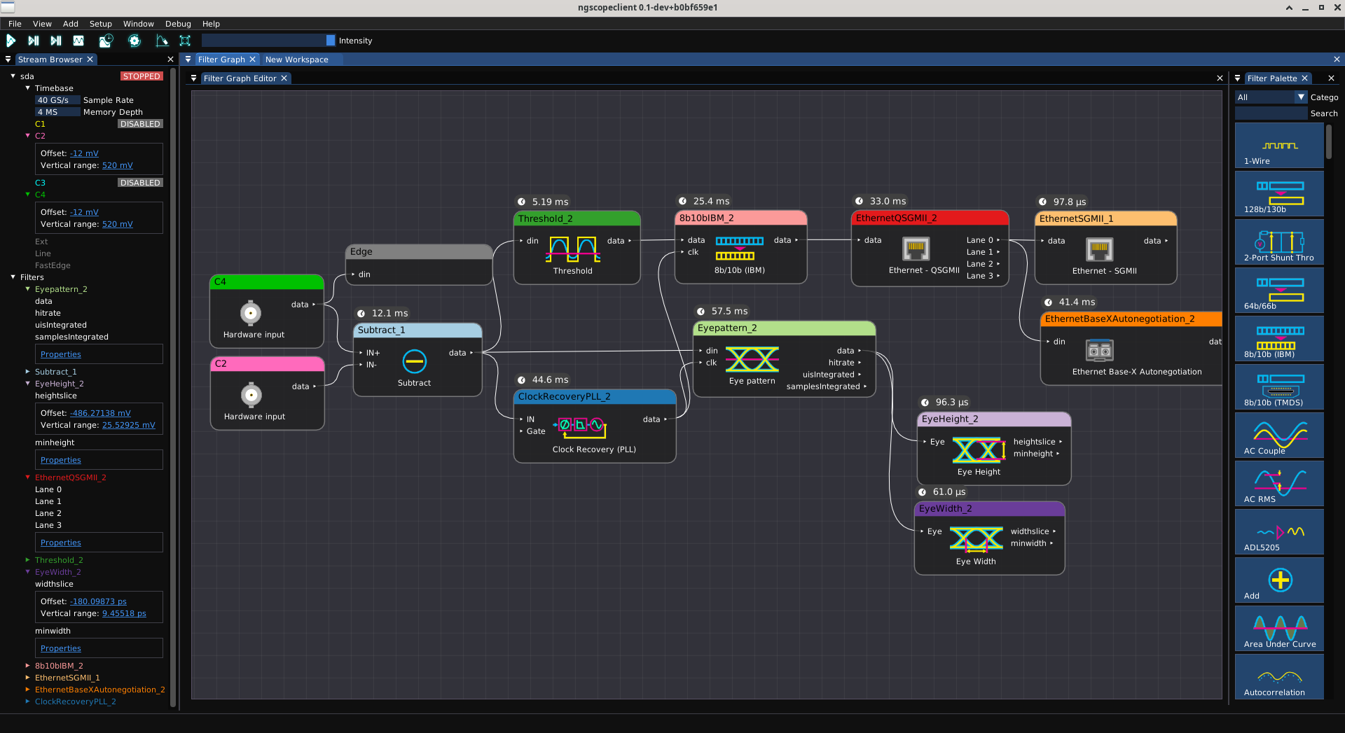
The filter graph shows the processing being performed on the raw scope waveforms for this analysis. It’s so much easier to follow filter graphs now that we have pretty icons for at least most of the processing blocks. Thanks again to pirate, tetrikitty, and all of the other artists!
Ethernet MDI
As of now, I haven’t done proper SI measurements on the baseT links, but it links up and works with no bit errors during testing to date. At some point before I deploy the switch in prod I might generate and measure some compliance patterns but I have zero concerns based on other testing to date.
Thermals
On my bench now, using a low profile heatsink with 12mm fin height (Wakefield-Vette 960-27-12-D-AB-0) and a 40mm fan blowing generally down the line card’s axis but with no airflow ducting, temperatures are:
- PCB near PHY 0: 27.8C
- On die PHY 0: 39.5C
- PCB near PHY 1: 36.3C
- On die PHY 1: 60.9C
- PCB in power supply area: 30.2C
These are acceptable but definitely on the high end, especially for PHY 1 (right side as seen from the front panel, furthest from the fan), especially considering it’s sitting on a bench and not marinating in an enclosed 1U chassis.
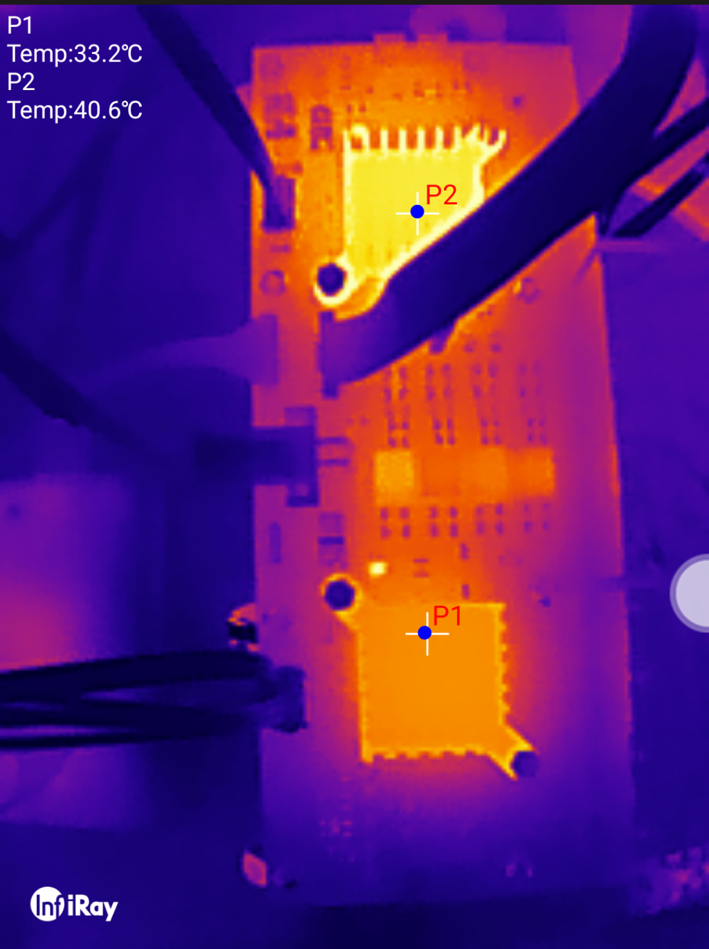
In thermal imagery (not calibrated for heatsink emissivity) the PHY heatsinks measure as 33.2 and 40.6C, with the PHY further from the fan - and the entire PCB area around it - visibly warmer. Also interesting is that the DC-DC module for the 2V5 rail (the highest output current) is slightly warmer than the others.
I plan to add some 3D printed air ducting to the actual switch chassis to ensure better control of flow paths and sufficient cooling for the PHYs, as well as swapping the 12mm tall heatsinks for the 23mm version which will dump heat far more effectively. Once the final hardware has been prototyped we’ll see how it performs.
Conclusions
The line card is working great and I don’t see any reason to make significant changes to it. This isn’t too surprising considering that much of the architecture was proven out on LATENTPINK a year or two ago, but I had to make sure everything was good before I spent a bunch of time and money populating more of them.
I did find one bug during the bringup process, however: the right LED on each port is swapped with the one above it (so for example if you plug a 10/100 device into the bottom left port, the top left port’s right LED will turn yellow). Rather than respinning the board, I decided to just fix this in software by using the GPIO bitbang mode on the PHY that lets me set the LED state over the MDIO bus. I don’t need fast response since the right LED just indicates <1 Gbps mode, while the left LED is the link up/traffic indicator and remains driven by the hardware since it’s hooked up correctly.
Like this post? Drop me a comment on Mastodon

![The 8pen input method for phones (2010) [video]](https://www.youtube.com/img/desktop/supported_browsers/edgium.png)

