.png)

This document is a complement to the README in the Github repository. The README provides information about performance, capabilities, and tests. This document reflects more on the why and how OrthoRoute was developed.
Video Intro
Project Overview
OrthoRoute is a GPU-accelerated PCB autorouter, designed for parallel routing of massive circuit boards. Unlike most autorouters such as Altium Situs, FreeRouting, and a dozen EE-focused B2B SaaS startups, OrthoRoute uses GPUs for parallelizing the task of connecting pads with traces.
The main focus of OrthoRoute is a unique routing technique borrowed from FPGA fabric routers. Instead of drawing individual traces, it first creates a 3-dimensional lattice of traces on multiple layers. Algorithms borrowed from the FPGA and VLSI world are used to connect individual pads. Unlike push-and-shove routers, OrthoRoute pre-lays a Manhattan lattice and uses a negotiated-congestion router (PathFinder) to produce valid connections for all nets.
OrthoRoute is designed as a KiCad plugin, and heavily leverages the new KiCad IPC API and kicad-python bindings for the IPC API.
Key Features:
- It’s a KiCad Plugin: Just download and install with the Plugin Manager
- Real-time Visualization: Interactive 2D board view with zoom, pan, and layer controls
- Professional Interface: Clean PyQt6-based interface with KiCad color themes
- GPU-Accelerated Routing: Routing algorithms in CUDA
- Multi-algorithm routing: Some boards are better suited to different algorithms
- Manhattan Routing: A grid of traces, vertical on one layer, horizontal on the other
- Lee’s Algorithm: Also, a traditional push-and-shove router (experimental)
But Why?
This is a project born out of necessity. Another thing I was working on needed an enormous backplane. A PCB with sixteen connectors, with 1,100 pins on each connector. That’s 17,600 individual pads, and 8,192 airwires that need to be routed. Here, just take a look:
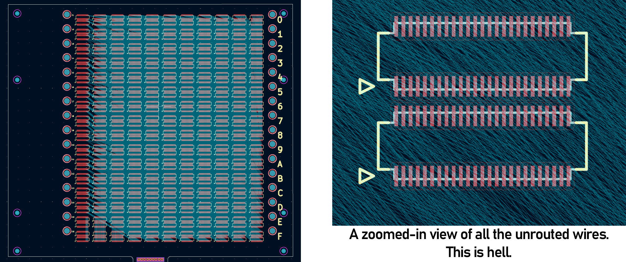
Look at that shit. Hand routing this would take months. For a laugh, I tried FreeRouting, the KiCad autorouter plugin, and it routed 4% of the traces in seven hours. If that trend held, which it wouldn’t, that would be a month of autorouting. And it probably wouldn’t work in the end. I had a few options, all of which would take far too long
- I could route the board by hand. This would be painful and take months, but I would get a good-looking board at the end.
- I could YOLO everything and just let the FreeRouting autorouter handle it. It would take weeks, because the first traces are easy, the last traces take the longest. This would result in an ugly board.
- I could spend a month or two building my own autorouter plugin for KiCad. I have a fairly powerful GPU and I thought routing a PCB is a very parallel problem. I could also implement my own routing algorithms to make the finished product look good.
When confronted with a task that will take months, always choose the more interesting path.
Screenshots
The Why and How of OrthoRoute
With the explanation of what OrthoRoute is out of the way, I’d like to dive into the How and Why of what this is. The following are the implementation details of OrthoRoute. How I built it, and why I made the decisions I did.
A New KiCad API and Implementation
KiCad, Pre-version 9.0, had a SWIG-based plugin system. There are serious deficits with this SWIG-based system compared to the new IPC plugin system released with KiCad 9. The SWIG-based system was locked to the Python environment bundled with KiCad. Process isolation, threading, and performance constraints were a problem. Doing GPU programming with CuPy or PyTorch, while not impossible, is difficult.
The new IPC plugin system for KiCad is a godsend. The basic structure of the OrthoRoute plugin looks something like this:
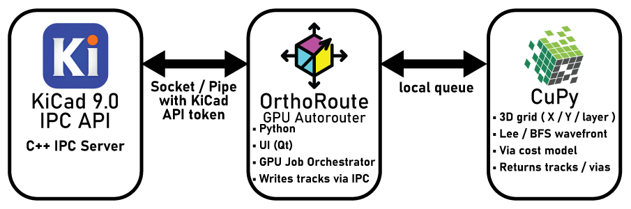
The OrthoRoute plugin communicates with KiCad via the IPC API over a UNIX-ey socket. This API is basically a bunch of C++ classes that gives me access to board data – nets, pads, copper pour geometry, airwires, and everything else. This allows me to build a second model of a PCB inside a Python script and model it however I want. With a second model of a board inside my plugin, all I have to do is draw the rest of the owl.
Why A GPU-Accelerated Autorouter Is Dumb
Before digging into the development of two separate autorouting engines, I’d first like to explain why building an autorouter for a GPU is a dumb idea. I’m going to explain this first because this specific insight plagued the development of both routing engines.
Autorouters are an inherently unparallizable problem. Instead of mapping an entire (blank) PCB into a GPU’s memory and drawing traces around obstacles, an autorouter is about finding a path under constraints that are always changing. If you have three nets, route(A→B), route(C→D), and route(E→F), you start out by routing the direct path (A→B). But (C→D) can’t take the direct path between those points, because it’s blocked by (A→B). Now (E→F) is blocked by both previous routes, so it takes a worse path.
It's _like_ the traveling salesman problem, but all the salesmen can't take the same road. Also there are thousands of salesmen. Should net (A→B) be higher priority than (C→D)? GPUs hate branching logic. You can't route (C→D) until you've routed (A→B), so that embarrassingly parallel problem is actually pretty small. Now deal with Design Rules. If you don't want a trace to intersect another trace of a different net, you apply the design rules. But this changes when you go to the next net! You're constantly redefining whatever area you can route in because of Design Rules, which kills any GPU efficiency.
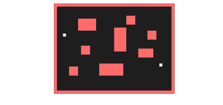 Wavefront expansion. The breadth-first search that finds the shortest path to a goal.
But all is not lost. There’s exactly one part of autorouting that’s actually parallel, and a useful case to deploy a GPU. Lee’s Wavefront expansion. You route your traces on a fine-pitch grid, and propagate a ‘wave’ through the grid. Each cell in the wave can be processed independently. Shortest path wins, put your trace there. That’s what I’m using the GPU for, and the CPU for everything else. Yeah, it’s faster, but it’s not great. Never trust the autorouter, but at least this one is fast.
Bug-finding and Path-finding.
After using the IPC API to extract the board, I had everything. Drills, pads, and copper pours. The next step was to implement path finding. This is the process of selecting an airwire, and finding a path between its beginning and end. This is what autorouters do, so I’m using standard algorithms like Wavefront expansion, and a few other things I picked up from a VLSI textbook. All I needed to do was convert that list of pads and traces and keepouts to a map of where the autorouter could draw traces.
The key insight here, and I think this is pretty damn smart, is that a copper ground plane is the map of where traces can go. If I create a board with a few parts on it and put down a ground plane, that ground plane defines where the autorouter can draw traces.
While the kicad-python library has functions that will return the polygon of a copper pour, I can’t use that. Not all boards will have a copper pour. What I really need to do is reverse engineer the process of making these copper pours myself. I need a way to extract the pads, traces, and keepouts and applying DRC constraints to them.
That’s exactly what I did. First I learned how to extract the copper pour from a board, giving me a 5000-point polygon of copper with holes representing pads, traces, and clearances. Then, I reverse engineered this to create a ‘virtual’ copper pour – one that could be generated even if the KiCad board file doesn’t have a copper pour. By comparing this ‘virtual’ copper pour to the ground truth of the copper pour polygon extracted from the board, I could validate that my ‘virtual’ copper pour was correct. This gives me an exact map of where the autorouter can lay down copper.
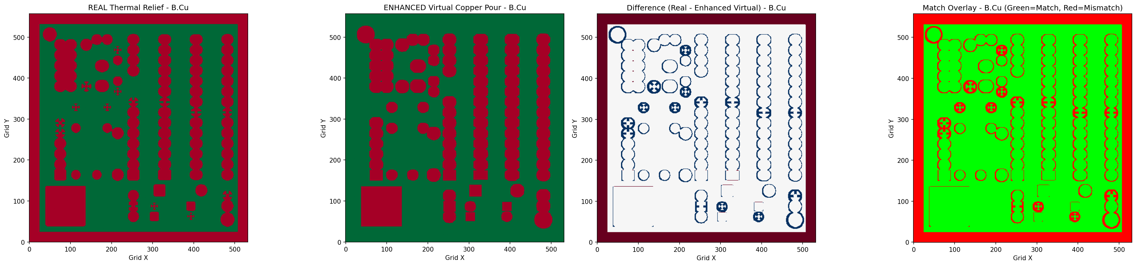
Pathfinding wasn’t the issue. There are standard algorithms for that. What really gave me a lot of trouble is figuring out where the pathfinding was valid. I’m sure someone else would have spent months going through IPC specifications to figure out where an autorouter should route traces. But I leveraged the simple fact that this data is already generated by KiCad – the copper pour itself – and just replicated it.
If there are any KiCad devs out there reading this, please implement a get_free_routing_space(int copper_layer) function in the next iteration kicad-python. Something that returns the polygon of a copper pour on boards that don’t have a copper pour, for each layer of copper.
The Non-Orthogonal Router
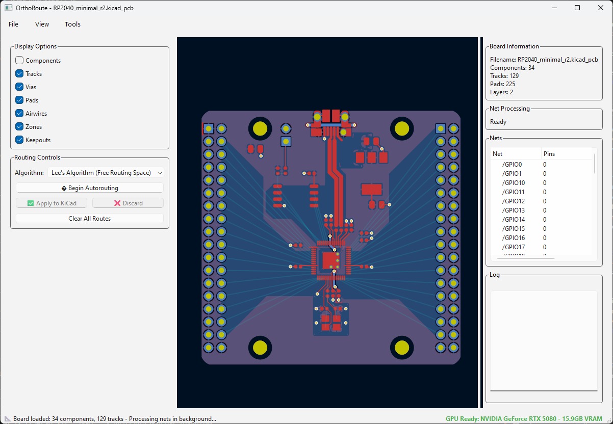
With that said, it’s time to show off what the KiCad IPC API can do. I chose to build a general purpose autorouter. Nothing fancy; just something that would route a few microcontroller breakout boards and a mechanical keyboard PCB. That’s exactly what I did. I built an autorouter that only uses wavefront expansion. And I quickly hit the fundamental limit of how useful this autorouter could be:
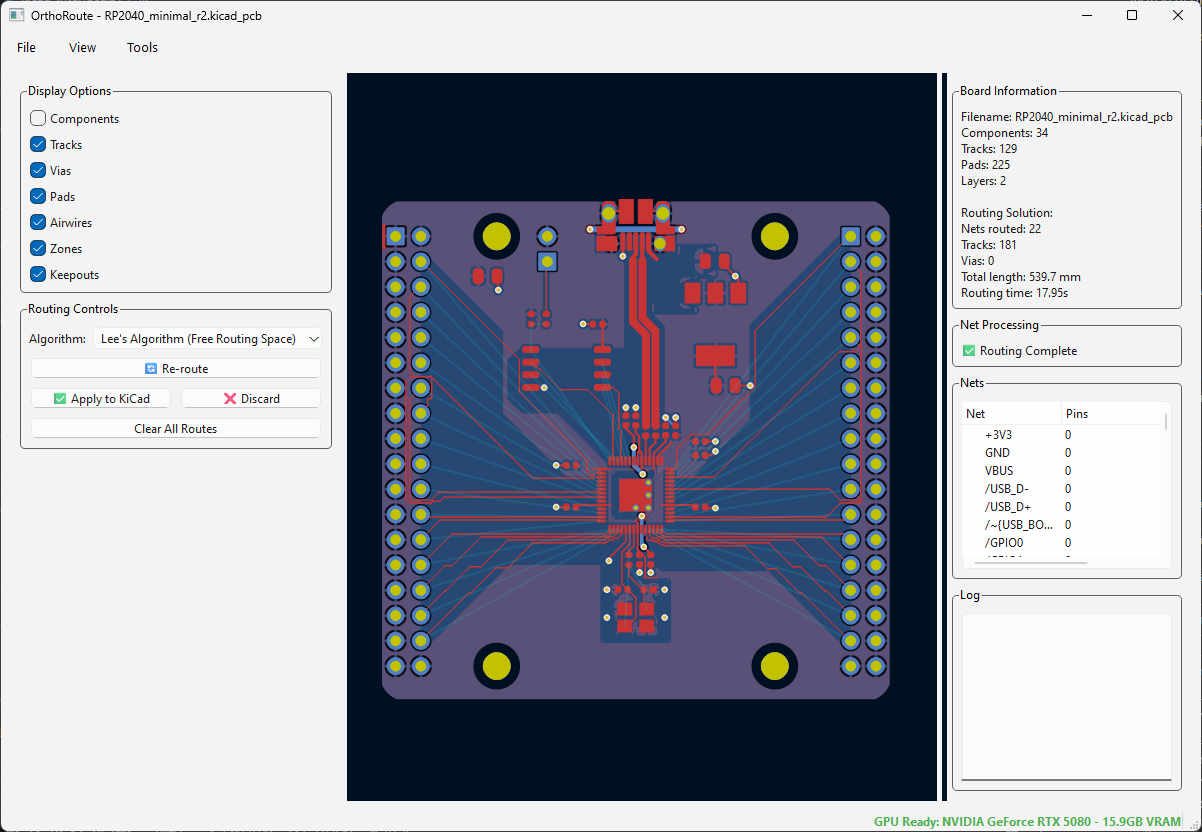
Above is a screenshot of the OrthoRoute plugin, attempting to route a board with an RP2040 microcontroller. This is the standard RP2040 breakout taken off of Raspberry Pi’s FTP server. I deleted the traces that put the GPIOs onto pin headers and pressed ‘Route Now’. The results were terrible.
This is routing with DRC awareness if you look really close. The routed traces aren’t interfering with each other, but not many traces are routed. Airwires are still there, and the routing isn’t quite as good as it could be.
For a single pass, this is fine! But autorouters don’t do a single pass. There are other techniques not implemented in this plugin like:
- Push-and-Shove routing. This technique moves existing traces to make room for new ones. It’s found in all real autorouters, but not implemented here
- Rip-up and retry. Right now we have single-pass routing. If a route fails, it’s done. Rip-up is the ability to remove ‘blocking’ or conflicting routes and try alternate paths.
- A global routing plan. When a person looks at a circuit board full of airwires, they might see ‘busses’ – a bunch of traces that all go from one component to another. It would be really smart to route these together, and route these first. I’m not doing that with my OrthoRoute. I’m just grabbing the first net from a list of unrouted nets and routing that.
But a traditional autorouter isn’t the point here
Development of this traditional autorouter stalled. Primarily for a good reason: my initial attempts at building this ‘non-orthogonal’ router were plagued by intersecting traces. The routing appeared to be not DRC aware. This was fixed when I realized what the problem was. Because I was routing in parallel batches (I’m using a GPU, so why not), routing one net did not take into account the other nets that were being routed at the same time. This resulted in different nets with intersecting traces and would fail DRC if it was ever pulled into KiCad.
The solution to this was to route the nets sequentially. I could still use the GPU for pathfinding, but routing multiple nets at the same time simply wouldn’t work. Either way, this ‘non-orthogonal router’ was just a test to see if I could actually pull this off. I’m only doing this project to route my pathological backplane, anyway.
Development of the Manhattan Routing Engine
With the ability to read and write board information to and from KiCad, and some GPU autorouting experience under my belt, I had to figure out a way to route this stupidly complex backplane. A non-orthogonal autorouter is a good starting point, but I simply used that as an exercise to wrap my head around the KiCad IPC API. The real build is a ‘Manhattan Orthogonal Routing Engine’, the tool needed to route my mess of a backplane.
Obviously a traditional push-and-shove autorouter wouldn’t work well, and I wanted something fast. The solution to both of these problems is to pre-define a ‘grid’ or ‘lattice’ of traces, with only vertical traces on the top-most layer, only horizontal traces on the next layer down. This would continue vertical traces on the layer below that, alternating horzontal and vertical for the entire board stack.
To route a trace through this lattice, I first take a signal or airwire off a pad, and design a ‘pad escape route’ that ends in a via and ‘punches down’ into the grid. From here, it’s routing through a Manhattan-like grid; a well-studied problem in computer science.
The algorithm I’m using is the eminently ungooglable PathFinder algorithm. This is an algorithm designed for routing FPGA fabric. The algorithm assumes an orthogonal grid and routes points to point in an iterative process. The first pass is lazy and greedy so there’s a lot of congestion on certain edges of a graph. For a PCB, this means multiple nets run over the same physical trace. After each iteration, this congestion is measured and routing begins again. Eventually the algorithm converges on a solution that’s close to ideal.
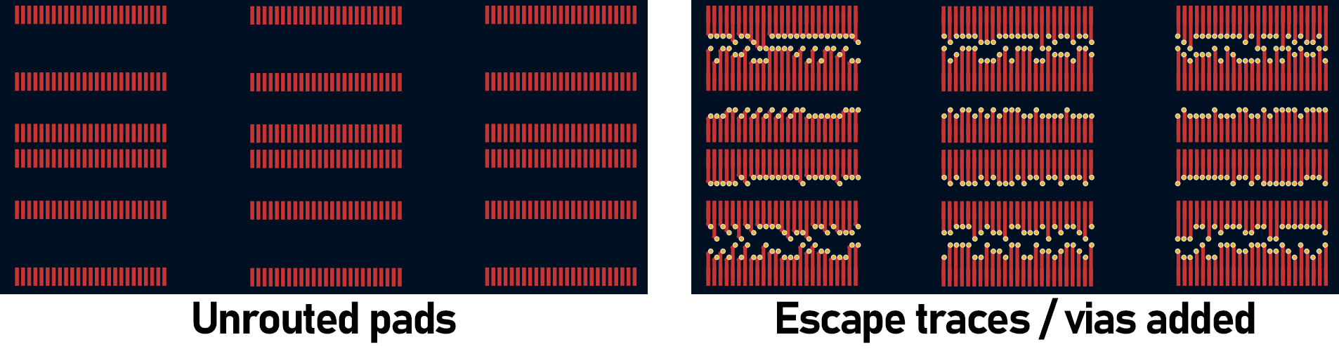
The first step of that is the pad escape planner that pre-computes the escape routing of all the pads. Because the entire Manhattan Routing Engine is designed for a backplane, we can make some assumptions: All of the components are going to be SMD, because THT parts would kill the efficiency of a routing lattice. The components are going to be arranged on a grid, and just to be nice I’d like some ‘randomization’ in where it puts the vias punching down into the grid. Here’s what the escape planning looks like:
For a 100mm x 100mm board with four routing layers and a 0.4mm pitch, we’re looking at approximately 250 nodes in each direction, which is 62,500 nodes per layer. Multiply that by four layers and we have 250,000 nodes in our graph. Each node can connect to up to six neighbors (four in-plane directions plus up and down through vias), giving us roughly 1.5 million edges. This is where the GPU comes in handy.
PathFinder works in iterations. In the first pass, each net routes itself greedily through the lattice, completely ignoring every other net. This is fast and gets everything connected, but results in massive congestion – dozens of nets might be sharing the same physical trace segment. After the first iteration, we calculate a cost function for every edge in the graph. Edges with more congestion get higher costs. In the next iteration, nets route themselves again, but this time they avoid the expensive (congested) edges when possible. Nets that caused the most problems get “ripped up” and re-routed first, forcing them to find alternative paths.
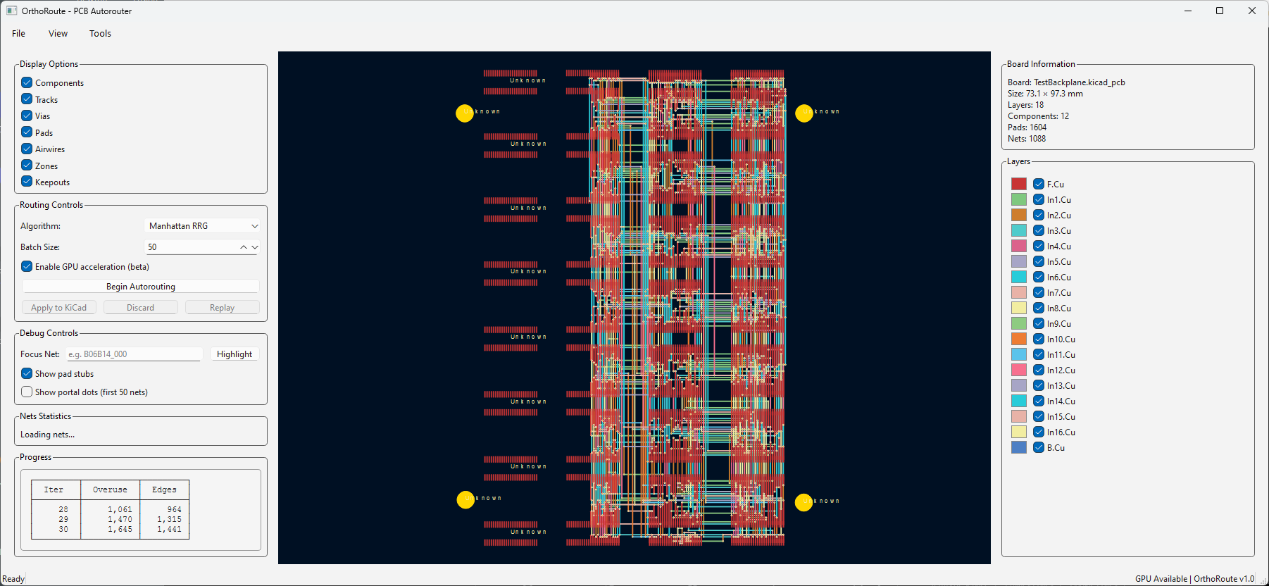
This process repeats. With each iteration, congestion decreases as nets find less contested paths through the lattice. The algorithm typically converges to a valid, uncontested solution within 5-10 iterations for most boards. For that massive 17,600 pad backplane? It routes in minutes on an RTX 5080.
After a few months of work, I was hitting a wall. I could route through this grid, traces were appearing, but it just couldn’t finish routing. On a small test board, about 270 out of 512 nets would route; the rest would be inexplicably trapped, somehow. That’s when I remembered by problems with the traditional push-and-shove router. Because I was routing nets in parallel, they would self-intersect and thus fail the checks for different nets overlapping. My PathFinder implementation routed nets in batches, in parallel. Because these nets committed their position to the graph at the same time, they would always fail. PathFinder is, at its heart, a sequential algorithm. There aren’t many tricks you can use to parallelize a PathFinder autorouter.
The same bug hit me again – autorouting is an inherently sequential algorithm. Lesson learned.
But with that fixed, I got iterations of PathFinder eventually converging, giving me these DRC-correct board layouts:
Why PathFinder Kinda Sucks for PCBs
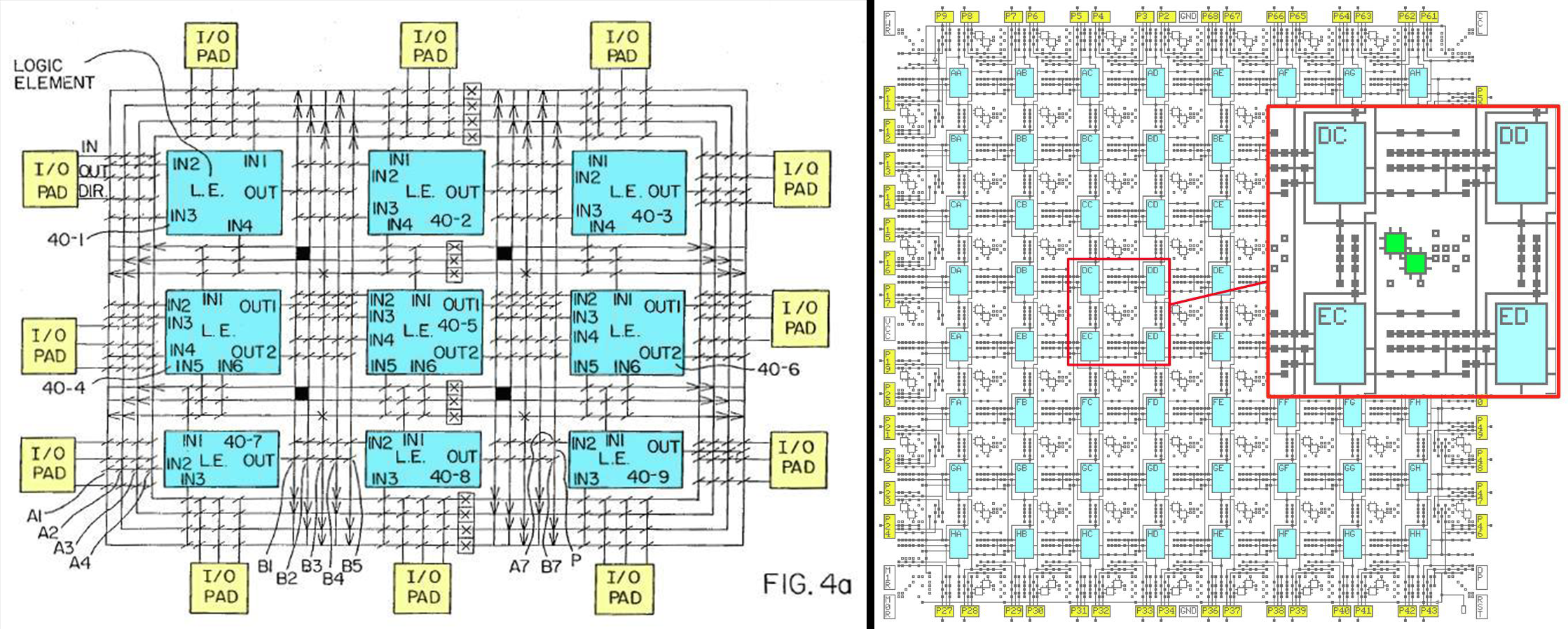
The original PathFinder paper was, “A Negotiation-Based Performance-Driven Router for FPGAs” and from 1995, this meant early FPGAs like the Xilinx 3000 series and others manufactured by Tryptych. These devices were simple, and to get a good idea of how they worked, check out Ken Shirriff’s blog. Here’s what the inside of a Xilinx XC2064 looks like:
The basic idea behind this FPGA is that there are blocks, and you route between them with an orthogonal grid. The PathFinder algorithm works something like this: total_cost = base_cost + pres_fac × current_congestion + hist_weight × historical_congestion
The PathFinder algorithm is extremely sensitive to these history costs, pressure factors, congestion, and a dozen other parameters that control how aggressively the route negotiates between competing nets and between iterations of the algorithm.
For FPGAs, this isn’t a problem, because you can tune the parameters in the lab and every other routing task for that specific FPGA will also converge. You’re routing within a fixed, well characterized architecture. But everyone can make a PCB. Will the same parameters used on a 4-layer Arduino clone work on a 24-layer backplane? No.
When PathFinding an FPGA, you know the constraints of that specific FPGA’s fabric. When PathFinding a circuit board, all the constraints must be derived.
How PathFinder Almost Killed Me
While developing OrthoRoute, I found every failure mode possible. The router would start fine with 9,495 edges with congestion in iteration 1. Then iteration 2: 18,636 edges. Iteration 3: 36,998 edges. The overuse was growing by 3× per iteration instead of converging. Something was fundamentally broken.
The culprit? History costs were decaying instead of accumulating. The algorithm needs to remember which edges were problematic in past iterations, but my implementation had history_decay=0.995, so it was forgetting 0.5% of the problem every iteration. By iteration 10, it had forgotten everything. No memory = no learning = explosion.
With the history fixed, I ran another test. I got oscillation. The algorithm would improve for 12 iterations (9,495 → 5,527, a 42% improvement!), then spike back to 11,817, then drop to 7,252, then spike to 14,000. The pattern repeated forever. The problem was “adaptive hotset sizing”—when progress slowed, the algorithm would enlarge the set of nets being rerouted from 150 to 225, causing massive disruption. Fixing the hotset at 100 nets eliminated the oscillation.
Even with fixed hotsets, late-stage oscillation returned after iteration 15. Why? The present cost factor escalates exponentially: pres_fac = 1.15^iteration. By iteration 19, present cost was 12.4× stronger than iteration 1, completely overwhelming history (which grows linearly). The solution: cap pres_fac_max=8.0 to keep history competitive throughout convergence.
With all fixes in place, a 30-layer board with 512 nets converged to zero overuse at iteration 21. Success!
Then I tested a 12-layer board. Complete failure: 493/512 nets routed, 14,300 overuse across 4,648 edges, stalled at iteration 40. Same code, same parameters, different board.
How I made PathFinder not suck
PathFinder is designed for FPGAs, and each and every Xilinx XC3000 chip is the same as every other XC3000 chip. Every single PCB is different from every other PCB. What I had to do was figure out these paramaters on the fly. So that’s what I did. Right now I’m using Board-adaptive parameters for the Manhattan router. Before beginning the PathFinder algorithm it analyzes the board in KiCad for the number of signal layers, how many nets will be routed, and how dense the set of nets are. It’s clunky, but it kinda works.
Where PathFinder was tuned once for each family of FPGAs, I’m auto-tuning it for the entire class of circuit boards. A huge backplane gets careful routing and an Arduino clone gets fast, aggressive routing. The hope is that both will converge – produce a valid routing solution – and maybe that works. Maybe it doesn’t. There’s still more work to do.
The Future of OrthoRoute
I built this for one reason: to route my pathologically large backplane. Mission accomplished. And along the way, I accidentally built something more useful than I expected.
OrthoRoute proves that GPU-accelerated routing isn’t just theoretical, and that algorithms designed for routing FPGAs can be adapted to the more general class of circuit boards. It’s fast, too. The Manhattan lattice approach handles high-density designs that make traditional autorouters choke. And the PathFinder implementation converges in minutes on boards that would take hours or days with CPU-based approaches.
More importantly, the architecture is modular. The hard parts—KiCad IPC integration, GPU acceleration framework, DRC-aware routing space generation are done. Adding new routing strategies on top of this foundation is straightforward. Someone could implement different algorithms, optimize for specific board types, or extend it to handle flex PCBs.
The code is up on GitHub. I’m genuinely curious what other people will do with it. Want to add different routing strategies? Optimize for RF boards? Extend it to flex PCBs? PRs welcome, contributors welcome.
And yes, you should still manually route critical signals. But for dense digital boards with hundreds of mundane power and data nets? Let the GPU handle it while you grab coffee. That’s what autorouters are for.
Never trust the autorouter. But at least this one is fast.


