.png)

Main
Solving matrix equations Ax = b is central to linear algebra and applications such as signal processing1,2, scientific computing3 and second-order training of neural networks4,5 (Fig. 1a). In scientific computing, differential equations with continuous variables are converted into matrix equations with discretized variables6. When solving inverse problems, the outputs are more sensitive to input errors than in regular forward matrix multiplication, and thus, high-precision computing is required. However, achieving high precision with digital methods is computationally expensive, often requiring operations with polynomial complexity (such as O(N3), where N is the matrix size). With the rise of applications using vast amounts of data, this creates a challenge for digital computers, particularly as traditional device scaling becomes increasingly challenging7. In addition, the separation of processor and memory in the conventional von Neumann architecture creates a bottleneck for data-intensive computations, further limiting performance and efficiency8.
Analogue matrix computing (AMC) with resistive memory arrays can be used to accelerate the solving of matrix equations9. A resistive memory array can be viewed as a physical matrix, where the conductance of each device is treated as an element of the matrix. As matrix–vector multiplication (MVM) is the dominant operation in solving matrix equations, replacing the digital synthesis of the MVM process with a single resistive memory array (Fig. 1b) should drastically reduce computational complexity10,11, and an isolated array with grounded rows has been used to perform MVM in one step12. This approach is, however, still limited by discrete iterations and by the conversion between the analogue and digital domains.
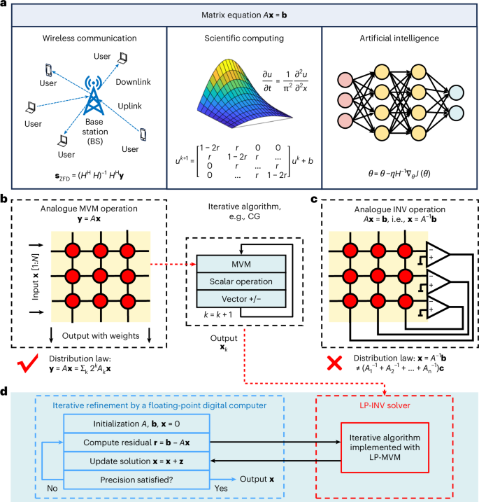
a, Representative applications of solving the INV equation, including signal processing in wireless communications, differential equation solving in scientific computing and neural network training in artificial intelligence. b, MVM-based iterative algorithm for solving the INV equation. The resistive memory array-based AMC circuit can perform an MVM operation in one step. The algorithm also applies some scalar and vector operations. For high-precision solving, bit-slicing can be used by combing the partial results from several MVM circuits, thanks to the distributive law in MVM. c, The resistive memory array-based closed-loop circuit for solving the INV equation in one step. However, because of the deficiency of the distributive law in INV, improving the precision is challenging. d, Mixed-precision approach for solving the INV equation. This is an iterative refinement algorithm, where the digital computer refines the solution accuracy and the resistive memory array is used to implement the iterative MVM-based solver, with the help of, again, the digital computer.
By setting up closed-loop feedback between the resistive memory array and traditional analogue components, such as operational amplifiers (OPAs), the resulting circuit can solve matrix inversions (INVs) in one step, without the need for iterations13 (Fig. 1c). This concept has been extended to a range of matrix equations14,15,16,17,18,19,20. The computing process has also been shown to have no dependence on matrix size, as the computational complexity within a single array is reduced to a minimum21. The in situ computing property of AMC with resistive memory can also help overcome the von Neumann bottleneck, thus enhancing computing throughput and energy efficiency22.
Despite the potential of this closed-loop analogue approach, its low precision remains an issue. Furthermore, the hard wiring of the circuit also creates challenges for the scalability of the approach. In analogue MVM, the computing precision can be improved by combining several partial results using strategies including bit-slicing and analogue compensation23,24,25. Large-scale MVM operations can also be done by using several arrays to map block submatrices26,27,28. However, the lack of a distributive law and block matrix method in matrix equation solving makes it challenging to address the precision and scalability issues of analogue INV29.
One solution is to adopt an analogue–digital hybrid design30,31,32,33,34. Previous approaches have incorporated a low-precision iterative MVM-based analogue solver (Fig. 1b) in an iterative refinement algorithm35,36,37, where a floating-point digital computer is used to perform high-precision MVM (HP-MVM) operations that converge to an accurate result (Fig. 1d). However, this compromise diminishes the benefit of analogue computing in reducing complexity and requires analogue–digital conversion, resulting in only an incremental improvement in matrix equation solving performance. A natural upgrade to this scheme is to replace the iterative MVM-based solver with a one-step INV solver. However, analogue INV operations have been limited to small-scale circuits with passive resistive random-access memory (RRAM) arrays, which is not favoured for foundry fabrication and lacks reliable multilevel memory characteristics.
In this Article, we describe a high-precision matrix equation solving scheme that is based on fully analogue matrix operations. It uses iterative steps combining low-precision INV (LP-INV) and HP-MVM, thus preserving the inherent low complexity of AMC. In particular, the analogue INV reduces the number of iterations by providing an approximately correct result in every iteration. High-precision analogue MVM is achieved by bit-slicing23,24. We validate in hardware the BlockAMC method38, which solves large-scale matrix equations using block matrices, and use it to solve medium-scale (16 × 16) matrix equations. Our system uses high-performance RRAM chips that are fabricated in a foundry with a one-transistor-one-resistor (1T1R) cell structure in which each cell has eight conductance levels.
HP-INV scheme with analogue matrix operations
The high-precision INV (HP-INV) scheme is illustrated in Fig. 2a. It can be viewed as an iterative refinement algorithm, which, however, is implemented in the analogue domain. Both LP-INV and HP-MVM operations are performed using 1T1R RRAM circuits, configured with or without closed-loop feedback connections, respectively. Importantly, both INV and MVM are performed with well-defined bit resolution to adapt to multilevel memory technology. This contrasts with previous approaches that relied on stochastic approximate mapping, which is inconsistent with conventional memory operations39. High precision is possible in analogue computing only with a high-precision analogue representation of the model parameters40. For solving Ax = b, a high-precision copy of matrix A is provided for the MVM, which is implemented on a 1-Mb RRAM chip. During the iterations, the LP-INV provides the approximate initial solution and successive increments, whereas convergence to the target accuracy is ensured by HP-MVM. Specifically, matrix A, originally represented in floating-point form, is converted into fixed-point digits and sliced into several low-precision matrices: A = 20A0 + 2mA2 + ⋯ + 2(n−1)mAn−1. In our implementation, m = 3, and the resulting slice matrices are mapped into RRAM arrays. Because only 3 bits need to be written per device, the complexity of the hardware mapping is greatly reduced. Recent studies have used more conductance levels, such as >16 levels (equivalent to 4 bits), although this improvement comes at the cost of increased programming overhead41,42,43.
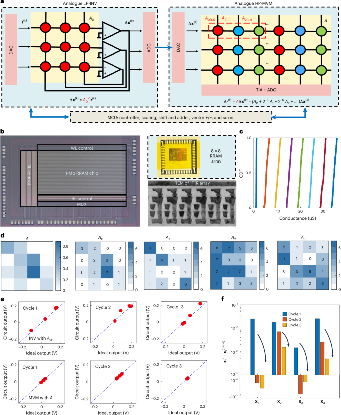
a, Schematic of the HP-INV scheme, which consists of iterations of LP-INV and HP-MVM operations, both of which are implemented by AMC circuits. After initialization, one time of low precision is completed, the result of which has an error due to inherent problems with the AMC circuit and which can be reduced by high-precision AMC MVM. By computing the residual error, we can judge whether a new cycle is required. A microcontroller unit manages the scaling of the matrix and vector parameters, the shift-and-add operations in HP-MVM, and the addition and subtraction of vectors. b, Photographs of foundry-fabricated TaOx-based RRAM chips: a 1-Mb chip for performing HP-MVM operations and an 8\(\times\)8 RRAM array used in the analogue INV circuit to perform LP-INV operations. The two chips were fabricated with the same process on a commercial 40-nm CMOS manufacturing platform. The memory cell adopts the 1T1R cell structure, as revealed by the cross-sectional transmission electron microscopy image. c, Cumulative distribution function plot of eight conductance states achieved with the write–verify method, which allows sufficient read-out margins. d, Example of high-precision solving of INV for a 4\(\times\)4 12-bit matrix A, including the bit-slicing results (A0–A3). The most significant matrix A0 is mapped in the LP-INV circuit, and all sliced matrices will be stored in the HP-MVM circuits. Note that the original matrix A was scaled to perform bit-slicing. e, Experimental results of three cycles of LP-INV and HP-MVM. The input vector is b = [0.05, 0, 0.05, 0.025]T. f, Convergence of the INV solution. BL, bit line; CDF, cumulative distribution function; MCU, microcontroller unit; SL, source line; TEM, transmission electron microscopy; TIA, transimpedance amplifier; WL, word line.
The most significant slice matrix A0 is mapped in an RRAM array, which is used to constructing the analogue LP-INV circuit. All slice matrices are mapped in several RRAM arrays for HP-MVM (Supplementary Fig. 1). In each iteration, the INV circuit computes the incremental results Δx(k) = A0−1r(k), where k is the cycle index, r(k) and Δx(k) are the circuit input and output, respectively. The initial input is r(0) = b, and the solution is updated as x(k+1) = x(k) + Δx(k+1) with x(0) = 0. Inputs are provided by digital-to-analogue converters (DACs), and outputs are digitized by analogue-to-digital converters (ADCs). Because the computation is approximate, low-resolution DACs and ADCs (for example, 4-bit) are sufficient. To refine the LP-INV result, the residual error r(k+1) = r(k) − Δr(k+1) = r(k) − AΔx(k+1) is evaluated using HP-MVM. Between LP-INV and HP-MVM operations, the addition, subtraction and scaling of vectors are also required. Scaling of the matrix and vectors is necessary to prevent unintended shifts in RRAM conductance states. HP-MVM of AΔx(k) is performed by bit-slicing (Supplementary Fig. 2), with slice matrices mapped to several arrays. The digitalized vector Δx(k) is likewise sliced and supplied through DACs. Each array executes low-precision MVM (LP-MVM), which produces partial results that are combined with shift-and-add operations to obtain the final output. The residual norm log2 ‖r(k)‖ is then compared with the tolerance 2−t. If the condition is not satisfied, the iterations continue until the desired precision is achieved. The pseudocode of the algorithm is provided in Supplementary Note 1.
Figure 2b shows photographs of the 1T1R RRAM chips used for the HP-INV demonstrations. An 8 × 8 array chip is configured as a closed-loop LP-INV circuit, and a 1-Mb RRAM chip performs HP-MVM, accommodating several slice matrices for bit-slicing operations. Unlike conventional memory arrays, the INV circuit requires feedback connections, which prevents the INV design from being scaled directly to the 1-Mb chip. The TaOx-based RRAM chips were fabricated on a commercial 40- nm complementary metal–oxide–semiconductor (CMOS) platform (Methods)44. The microstructure of the 1T1R array is shown in Fig. 2b. Results of current–voltage (I–V) switching characteristics, programming speed, state retention and recycling endurance are shown in Supplementary Figs. 3–6. Using the write–verify method (Methods)45, devices can be reliably programmed into eight conductance states spanning 0.5–35 μS, with sufficient read-out margins (Fig. 2c). Notably, 3-bit programming yields 100% success across 400 tested cells. The discrete conductance levels are used to encode slice matrices as 3-bit digits (000 to 111). The lowest state, obtained from a strong reset, represents numerical zero in the LP-INV circuit. To avoid a reliance on a strong reset, one more high-conductance state can be introduced, enabling a differential encoding scheme where the range from −7 to +7 is covered by state differences. This is a standard AMC approach for real-valued MVM. The full HP-INV solver system is shown in Supplementary Fig. 7. It comprises LP-INV and HP-MVM experimental set-ups controlled by a personal computer. The LP-INV circuit is implemented on a printed circuit board containing 8 × 8 RRAM arrays, OPAs, analogue switches, multiplexers (MUXs), DACs and ADCs. The HP-MVM set-up is a fully integrated chip composed of 1-Mb RRAM array, transimpedance amplifiers, ADCs, analogue switches, MUXs and registers (Methods).
An example of an HP-INV solution of a 4 × 4 positive matrix is shown in Fig. 2d–f. Matrix A was randomly generated and its elements truncated to 12-bit fixed-point numbers. The matrix was then sliced into matrices A0:3 (each with a different weight), which are stored in 3-bit RRAM arrays (Fig. 2d). Three cycles of analogue LP-INV and HP-MVM were performed in sequence, and the results are shown in Fig. 2e. After three cycles, the residual error of each element had reduced to the order of 10−3 (Fig. 2f). Each LP-INV operation exhibited remarkable errors, quantified by the relative error ‖v − v*‖/‖v*‖, where v* and v denote the ideal and experimental results, respectively. The average relative error of three LP-INV operations was 0.186, corresponding to a precision of only ~2.4 bits. Nevertheless, iterative refinement using updated residuals progressively improved the solution accuracy, as ensured by HP-MVM. The bit-sliced HP-MVM results are summarized in Supplementary Fig. 8. For the unsigned 12-bit matrix A and signed 12-bit input b, a total of 3 × (12/3) × (12/1) × 2 × 4 = 288 LP-MVM operations were performed, yielding 1,152 elements, each precisely correct.
When solving an INV equation, the condition number is an intrinsic factor that governs result precision, as it measures how input errors are amplified in the output. For the matrix A in Fig. 2d, the condition number κ = 7.7 yields a solution with a low precision of ~2.4 bits. For a better conditioned matrix (κ = 1.6), the LP-INV achieves ~4 bits or 5 bits of precision (Supplementary Fig. 9). Because the tailored matrix A0 is used in analogue INV solving, convergence requires that the spectral radius of I − AA0−1 be less than 1 (proof in Supplementary Note 2). HP-INV experimental results for matrices with various condition numbers (κ(A) = 2.5, 5, 33 and 34) are shown in Supplementary Fig. 10. Another factor affecting convergence is the programming error of A0, defined as the relative mapping error, ‖A0 − A0*‖/‖A0*‖, where A0 and A0* are the nominal and experimental matrices, respectively. In the experiment, the programming error was measured using a Keysight B1500A Semiconductor Parameter Analyzer with high-precision ADCs to ensure accurate conductance measurements and reliable error characterization. As shown in Supplementary Figs. 11 and 12, the convergence rate decreases as the relative mapping error increases. These factors contribute synergistically to determining the convergence rate.
HP-INV of real-valued and complex-valued matrices
The HP-INV approach can be extended to solving both real-valued and complex-valued matrix equations, which frequently arise in applications such as solving differential equations in scientific computing and signal processing in wireless communications. Several methods exist for real-valued analogue INV, including column-wise splitting with analogue inverters46 and row-wise splitting with conductance compensation47. The most convenient, however, is the bias-column method, which shifts the real-valued matrix by a constant: A = A+ − mJ = A+ − mjjT, where A+ is a positive matrix that can be mapped in an RRAM array, J is the all-ones matrix, j is the all-ones column vector and m is a coefficient controlling the shift magnitude. This method uses the same INV circuit as in Fig. 2a but requires one more row–column pair48. As the bias is usually fixed, it can be replaced with discrete resistors in the peripheral circuit. If the matrix is strictly diagonally dominant, the analogue INV can be further optimized by splitting off a diagonal term, which can also be implemented with resistors: A+ = Ap + nI, where Ap is a positive matrix mapped to the RRAM array, I is the identity matrix and n is a coefficient adjusting the diagonal. The resulting circuit for real-valued analogue INV is shown in Supplementary Fig. 13.
An example of a 4 × 4 real-valued matrix is shown in Fig. 3a. The matrix was randomly generated and truncated to 24-bit fixed-point representation. In this case, m = 0.4 and n = 2 were chosen to ensure the final matrix was positive for the LP-INV operation. HP-MVM was performed with the column-wise splitting scheme47. The convergence of the HP-INV solving process is shown in Fig. 3b. It achieves 24-bit precision after nine cycles. The precision of analogue INV is defined as the logarithm of the reciprocal of the relative error: log2 ‖v*‖/‖v − v*‖. From this definition, the HP-INV improves at a rate of ~3 bits per cycle, determined by the precision of the analogue LP-INV circuit.
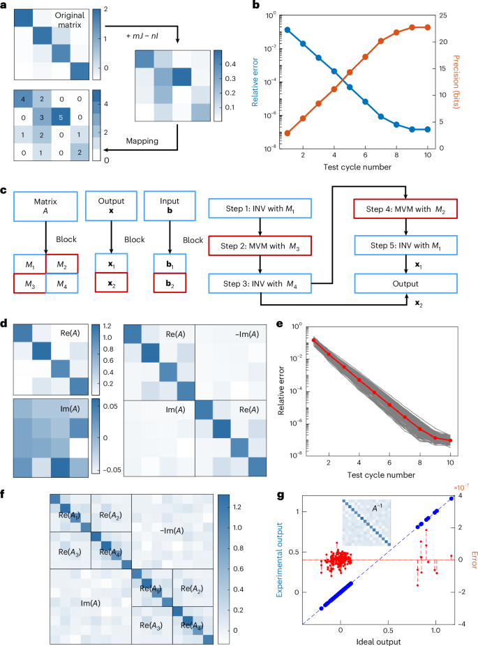
a, HP-INV results for a 24-bit 4 × 4 real-valued matrix. The original real-valued matrix is processed with the bias-column method (+mJ) to make all entries positive, where m is a coefficient for the shift magnitude and J is the all-ones matrix. For a diagonally dominant matrix, the off-the-diagonal operation can be performed, which makes the entries uniform when mapped to an RRAM array. b, Convergence of the HP-INV solving process. During the process, the precision increases by ~3 bits every cycle. At cycle 9, the solution reaches the maximum precision, 24 bits. The input vector is b = [0.1, 0.1, 0, −0.1]T. c, Explanation of the BlockAMC method. The original matrix is partitioned into four block submatrices, and the input and solution vectors are partitioned into two subvectors. The solution results are obtained at steps 3 and 5. d, A 24-bit 4 × 4 complex-valued matrix, which is converted into an 8 × 8 real-valued matrix. e, HP-INV results for the complex-valued matrix in d. Here 100 random tests were performed by randomly generating 100 input vectors. The red dots indicate the average convergence performance. At cycle 10, the solution results reach the maximum precision. f, A 24-bit 8 × 8 complex-valued matrix, which is converted into a 16 × 16 real-valued matrix. The original matrix is partitioned twice, into 4 × 4 block submatrices. The INV solution is obtained using the two-stage BlockAMC method. g, Results for inverting the 16 × 16 real-valued matrix (inset). The relative error is of the order of 10−7 after ten cycles of iteration. Altogether, 16 single HP-INV operations were performed in calculating the inverse matrix.
Solving complex-valued matrix equations typically involves converting them into real-valued matrices, where the real and imaginary parts, Re(A) and Im(A), form submatrices, doubling the matrix size. Analogue INV can naturally be combined with the BlockAMC scheme, which partitions a large matrix into blocks for scalable AMC-based solutions of linear systems38. The block matrices are distributed in different arrays, enabling INV or MVM operations without reprogramming. The workflow (Fig. 3c) relies on a sequence of INV and MVM operations with block submatrices to recover the original solution. Specifically, INV is performed with Re(A) and MVM with Im(A). In the original algorithm, a second INV would be required for Re(A) + Im(A) Re(A)−1 Im(A). However, due to the approximate nature of LP-INV in iterative refinement, this step can be simplified by reusing Re(A) instead (Supplementary Note 2). During HP-INV, each LP-INV is executed with BlockAMC, whereas HP-MVM is performed using bit-sliced submatrices. Intermediate results from Re(A) at steps 3 and 5 are combined to obtain the LP-INV solution of the expanded real-valued system. As an example, Fig. 3d shows a 4 × 4 complex-valued matrix expanded into the real-valued form \({\varOmega}_{A}=\left[\begin{array}{cc}{\rm{R}}{\rm{e}}(A) & -{\rm{I}}{\rm{m}}(A)\\ {\rm{I}}{\rm{m}}(A) & {\rm{R}}{\rm{e}}(A)\end{array}\right]\), so that this is equivalent to solving an 8 × 8 real-valued INV problem. The convergence of HP-INV is shown in Fig. 3e. Across 100 random input vectors, solutions generally reached 24-bit precision within ten cycles. Compared with the 4 × 4 real-valued case in Fig. 3a, one further cycle was required, reflecting the larger matrix size, the use of BlockAMC and the approximation with Re(A). Convergence precision is ultimately limited by the truncated precision of the matrix elements, as confirmed in Supplementary Fig. 14. Furthermore, as the two diagonal block matrices of ΩA are identical, that is, Re(A), the same circuit can perform both INV operations without reprogramming.
In BlockAMC, several stages of matrix partitioning can be applied to handle increasingly large matrices. In Fig. 3f, two-stage BlockAMC is used to solve the LP-INV of an 8 × 8 complex-valued (16 × 16 real-valued) matrix with 4 × 4 RRAM arrays. In the first stage, INV of Re(A) and MVM of Im(A) are performed. For the INV of Re(A), a second stage of BlockAMC partitions it into four blocks: Re(A1), Re(A2), Re(A3) and Re(A4). The intermediate results from INV of Re(A1) and Re(A4) are combined to recover the LP-INV solution of Re(A), and the two resulting vectors from INV of Re(A) at steps 3 and 5 in the first stage are combined to yield the LP-INV solution of the full 16 × 16 matrix. The workflow is illustrated in Supplementary Fig. 15. The inverse matrix of the 16 × 16 matrix was experimentally solved by performing 16 HP-INV operations, each with a column vector of the identity matrix as input. The convergence behaviour over ten cycles is shown in Supplementary Fig. 16. After ten cycles, the elements of the inverse matrix (Fig. 3g) match the ideal solution, with relative errors of the order of 10−7. These results clearly demonstrate the scalability of the analogue HP-INV solver for real-world applications.
Application of HP-INV to massive MIMO detection
Massive multi-input–multi-output (MIMO) technology is expected to substantially enhance the service quality of wireless communication systems in the 5G-A and 6G era49. In massive MIMO, the number of antennas at the base station (BS) is far greater than at the user equipment (UE; for example, a cell phone). The wireless channel is described by a matrix H of size M × K (M ≫ K). In the uplink (UE to BS), signal detection is required, whereas in the downlink (BS to UE), signal precoding may be applied. Both tasks are performed at the BS, where linear methods are commonly used that rely on the inversion of the matrix product HHH (with HH being the conjugate transpose of H) or on the generalized inverse of H. Because the matrix sizes in massive MIMO are moderate and can be readily accommodated in RRAM arrays, this problem is well suited to AMC circuits. This direction has recently attracted growing attention, but experimental demonstrations remain limited to small scales48,50, for example, 4 × 4 or 10 × 5. In addition, due to the limited precision of early AMC circuits, the modulation schemes tested have been restricted to 16-quadrature amplitude modulation (16-QAM), far from what is required in modern applications. Despite this, there is still a performance gap between AMC and digital processors. Here we demonstrate the HP-INV solver for massive MIMO detection with higher precision, larger matrix scales and higher-order modulation than previously reported48,50.
We first consider a 16 × 4 MIMO system. A binarized 100 × 100 image of the Peking University emblem is transmitted in the uplink and detected at the BS using the zero-forcing (ZF) method. In Fig. 4a, the binarized image is vectorized and encoded into a sequence of 256-QAM symbols (8-bit strings), grouped into four streams for transmission by four UE antennas. Each transmission delivers 32 bits of data to the BS. During modulation, each constellation point is encoded with a Gray code (Supplementary Fig. 17) to reduce the number of transmission errors51. The channel is modelled as Rayleigh fading52, where the elements of H follow a Gaussian distribution (Fig. 4a). In ZF detection, the received signal is recovered as s = (HHH)−1HHy, where y is the received vector and s is the recovered signal vector, which, ideally, is identical to the transmitted one. The most computationally demanding step is inverting the Gram matrix A = HHH, a known bottleneck for BS digital processors53. Here the HP-INV solver, assisted by one-stage BlockAMC, is used to invert the corresponding 8 × 8 real-valued matrix. The iterative results of image recovery are shown in Fig. 4b and constellation diagrams in Supplementary Fig. 18. Notably, after only two cycles, the transmitted image is reconstructed with full fidelity. As the binary image does not span the entire constellation space, uniformly generated samples were also tested to verify ZF detection performance. As shown in Fig. 4c, with just two HP-INV cycles, every constellation point is detected correctly without errors. These results demonstrate the precisely correct detection of massive MIMO with 256-QAM using AMC, thus addressing the long-standing precision bottleneck of analogue computing for reliable signal processing20,48,50,54. They also show that, despite its iterative nature, the HP-INV solver converges rapidly, thus minimizing the algorithmic overhead and supporting efficient signal detection.
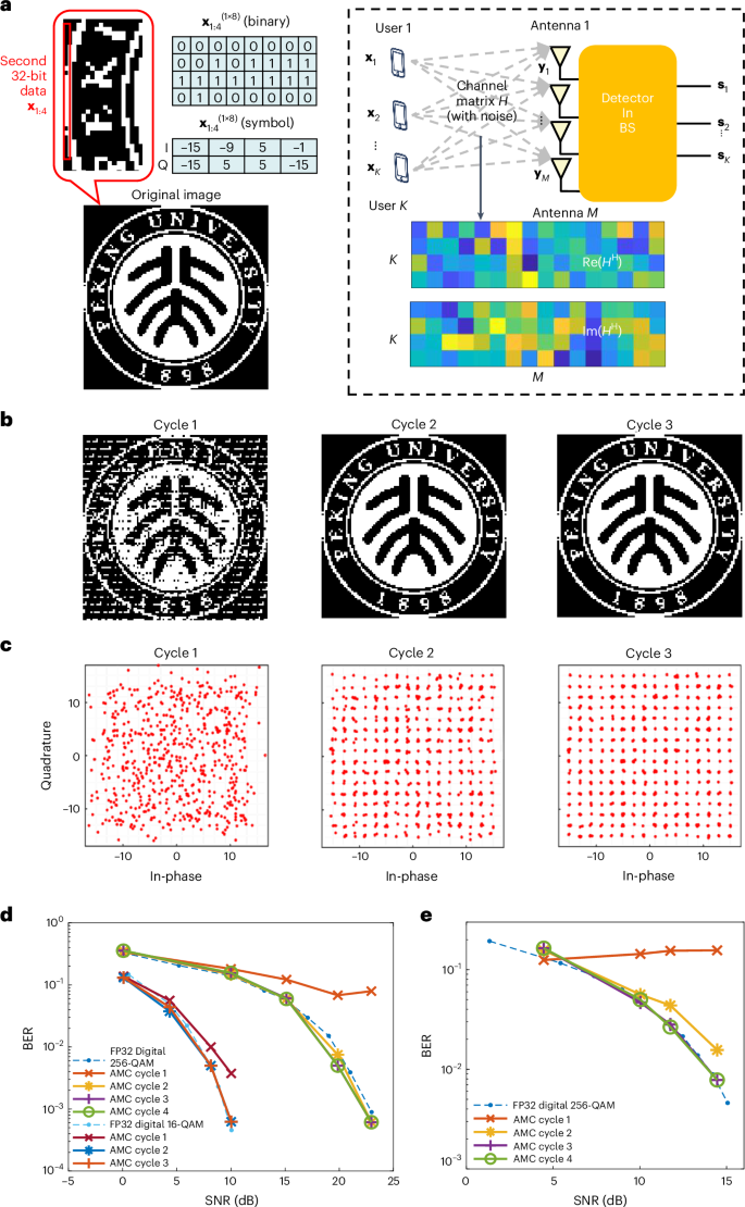
a, Illustration of a massive MIMO system with M BS antennas and K UE antennas. As an example, a 100 × 100 binarized image of the emblem of Peking University is transmitted in the uplink direction of a 16 × 4 MIMO. Each time, each UE antenna transmits 8 bits of binary data, which is equivalent to a 256-QAM symbol in the in-phase versus quadrature plane (I–Q). The signals are transmitted through a noisy channel and received at the BS, where the detection process recovers the QAM symbol. b, Images recovered by ZF detection. From left to right, the image is obtained by the vanilla analogue INV without iterative refinement, HP-INV with one cycle of iteration and HP-INV with two cycles of iteration. Notice that, at cycle 2, the received image is already the same as the original one. c, Constellation diagram for 644 256-QAM symbols recovered by ZF detection. The results are obtained in a similar way as b. The 644 symbols were uniformly generated for testing the performance of ZF detection with HP-INV. Also notice that, at cycle 2, all symbols are correctly detected with no errors. d, BER versus SNR curves for symbol transmission with 16 × 4 MIMO. The detection results from AMC and a FP32 digital processor are compared, for both 256-QAM and 16-QAM. The AMC results are obtained by HP-INV (or the vanilla INV circuit), in combination with BlockAMC. For both 256-QAM and 16-QAM, two cycles of HP-INV are sufficient to match the performance of the digital processor. e, BER versus SNR curves for symbol transmission with a 128 × 8 MIMO system. The AMC results are obtained and compared in the same way as those in d, but only 256-QAM is considered. The performance of HP-INV after three cycles is exactly the same as that of the FP32 digital processor.
To systematically evaluate the bit error rate (BER) versus signal-to-noise ratio (SNR), we randomly generated hundreds of sets of 256-QAM vectors uniformly distributed as U(0, 255) for the 16 × 4 massive MIMO system. Each element was transformed to a complex value using Gray coding. The SNR is defined as 20 × \({{\rm{l}}{\rm{o}}{\rm{g}}}_{10}\frac{{\parallel {\bf{y}}-\mathop{{\boldsymbol{n}}}\limits^{ \sim }\parallel }_{2}}{{\parallel \mathop{{\boldsymbol{n}}}\limits^{ \sim }\parallel }_{2}}\), where \(\parallel {\bf{y}}-\mathop{{\bf{n}}}\limits^{ \sim }{\parallel }_{2}\) and \(\parallel \mathop{{\bf{n}}}\limits^{ \sim }{\parallel }_{2}\) are the mean-square values of the signal and noise, respectively. Channel transmission was modelled as \({\bf{y}}=H{{\bf{s}}}_{{\bf{x}}}+\mathop{{\bf{n}}}\limits^{ \sim }\), where sx and y are the transmitted and received signals, respectively, and \(\mathop{{\bf{n}}}\limits^{ \sim }\) is an independent and identically distributed complex Gaussian noise vector with zero mean52. For completeness, we also evaluated 16-QAM. The BER results are shown in Fig. 4d, which compares the performance of HP-INV across iterations with that of 32-bit floating-point (FP32) digital computing. For 256-QAM, HP-INV achieves a BER comparable with that of the digital approach within only two cycles. At high SNR, the BER of HP-INV even surpasses that of the digital baseline, which is probably due to statistical fluctuations arising from the limited sampling. For 16-QAM, HP-INV also matches the digital performance within two cycles. Notably, although the BER of 256-QAM saturates at a high level after the first cycle, in 16-QAM it decreases steadily with SNR, indicating that lower precision is sufficient for the simpler modulation scheme.
The addressable size of massive MIMO can be scaled up using HP-INV with multistage BlockAMC. We applied a two-stage BlockAMC for signal detection in a 128 × 8 system, modulated with 256-QAM, by solving 8 × 8 complex-valued (16 × 16 real-valued) INV equations. The experimental test procedure was the same as for the 16 × 4 system, and Fig. 4e shows that HP-INV achieved the same performance within three cycles as an FP32 digital processor. These findings highlight the promise of combining HP-INV with BlockAMC to enable high-fidelity, efficient signal processing for massive MIMO in the 6G era.
Transient response and benchmarking of AMC
The key advantage of AMC is its extreme parallelism, which enables matrix equations to be solved in a single step. We experimentally measured the transient response of the analogue INV circuit. Five representative results are shown in Fig. 5a. The circuit converges within 120 ns for 4 × 4 matrices, demonstrating very high speed. As predicted by theory, the response depends on the gain–bandwidth product (GBWP) of the OPAs and on the smallest eigenvalue of the matrix, λmin, rather than on matrix size. Specifically, the time complexity is O((1/λmin) log(1/ϵ)), where ϵ is the demanded precision21. For certain cases, such as diagonally dominant matrices where λmin is nearly constant, the time complexity effectively reduces to O(1) (ref. 21). The situation for MVM is even simpler, as it is essentially a parallel read-out process of several memory cells, and the time complexity of a single MVM operation can also be considered as O(1). Although the response time of MVM is widely expected to reach ~10 ns (ref. 25), our experimental results are around 60 ns (Fig. 5b). With bit-slicing, several LP-MVM operations can be executed simultaneously owing to the distributive property of MVM. Together, these observations indicate that the speed of HP-INV is governed by the response times of individual INV and MVM operations and the number of iterations required.
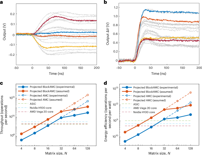
a, Transient curves of the LP-INV circuit. The matrix in the experiment is Re(A) in Fig. 4. Five individual input vectors were tested, resulting in 20 output curves. The average response time is about 120 ns. b, Transient curves of the MVM circuit. Again, 20 output curves were collected, and the average response time is about 60 ns. Red, INV output 1; blue, INV output 2; orange, INV output 3; yellow, INV output 4. c,d, Benchmarking of computing throughput (c) and energy efficiency (d) of AMC and state-of-the-art digital processors, namely two GPUs and one ASIC. The same computing precision (FP32) was maintained for all candidates.
The scalability of HP-INV arises from the BlockAMC mechanism, which should, however, lead to a non-constant complexity. We analysed the numbers of atomic INV and MVM operations needed in multistage BlockAMC. Assuming the atomic matrix size is N0, for an exponentially increasing matrix of size N, log2 N/N0 stages of BlockAMC are needed. As a result, the required number LP-INV of operations increases in proportion to \({\left(\frac{N}{{N}_{0}}\right)}^{{\log }_{2}3}\) and the number of HP-MVM operations increases as \({3\left(\frac{N}{{N}_{0}}\right)}^{2}-2{\left(\frac{N}{{N}_{0}}\right)}^{{\log }_{2}3}\). Although they asymptotically show complexities of O(N1.59) and O(N2), respectively, the scaling factor by 1/N0 greatly reduces the number of operations needed to solve real-world problems.
Based on a complexity analysis, we evaluated the scaling behaviour of the scalable HP-INV. As HP-INV can achieve the same precision as an FP32 digital processor, a direct performance comparison is appropriate. We considered a moderate array size of N0 = 32. BlockAMC is unnecessary below this size but required above it. A model for estimating the equivalent throughput and energy efficiency is provided in Supplementary Note 3. Both the solution time and energy dissipation include contributions from the LP-INV and HP-MVM modules, as well as DACs and ADCs. The throughput is estimated by calculating the equivalent number of digital operations and dividing by the measured solution time. For digital processors, INV and MVM scale with O(N3) and O(N2) complexity, respectively. Using experimental data on circuit response time and power consumption, Fig. 5c,d compares the scaling of HP-INV throughput and energy efficiency with that of standard digital processors: two graphics processing units (GPUs, Nvidia H100 and AMD Vega 20) and an application-specific integrated circuit (ASIC) designed for 128 × 8 massive MIMO signal processing55,56,57. Because GPU throughput scales linearly with core count, we normalize performance to that of a single core58,59. The energy efficiency is unaffected by this normalization. The ASIC design is particularly relevant, as the size of its target system matches our experimental case.
The results show that the throughput of digital processors (GPU cores and an ASIC chip) is consistently in the range of few giga floating-point operations per second (GFLOPS), which is reasonable given that all three are built with only a few million transistors. By contrast, the equivalent throughput of HP-INV increases cubically due to its constant complexity. At N0 = 32, the performance of HP-INV already surpasses that of all the digital processors. In the BlockAMC regime, performance growth slows but remains about ×10 higher than that of the digital processors at N = 128. The energy efficiency shows a similar trend: AMC outperforms all digital processors at N0 = 32 and is ×3–5 better at N = 128. If larger arrays could be directly supported for HP-INV without BlockAMC at N = 128, both throughput and energy efficiency would improve by roughly an order of magnitude. We have envisioned faster INV and MVM circuits, with response times of 20 ns and 10 ns, respectively, which may be achieved using advanced OPAs with a higher GBWP20. This benchmarking indicates that such improvements could yield a further ×4 gain in both throughput and efficiency. In the best case, AMC could, therefore, deliver up to three orders of magnitude higher throughput and nearly two orders of magnitude greater energy efficiency than digital processors.
We also evaluated the potential impact of wire resistance on the convergence rate of HP-INV. The resistance between two RRAM cells along a bit line or source line was estimated to be approximately 1.73 Ω. We simulated the HP-INV solving process for several LP-INV and HP-MVM cycles across matrix sizes from 4 × 4 to 128 × 128. The results, summarized in Supplementary Fig. 19 alongside results for ideal circuits without wire resistance, show that convergence remains highly consistent with the ideal case. Only a slight deviation is observed for the largest array (128 × 128), demonstrating the strong robustness of HP-INV to wire resistance. As a result, throughput and energy efficiency (Fig. 5c,d) are expected to remain largely unaffected.
The estimated results are encouraging. Compared with RRAM-based MVM applications, building large-scale INV circuits on-chip is more challenging, in that (1) the closed-loop circuit must be hard-wired, adding routing and layout complexity; (2) all rows and columns of the array must be activated simultaneously, producing large currents on the bit and source lines, whereas MVM needs to activate only a few lines at a time thanks to its distributive property; and (3) noise from circuit parasitics is amplified during the solving process. These factors limit the feasible array size of a single INV circuit. Nevertheless, as shown above, arrays of 32 × 32 to 64 × 64 can already deliver remarkable gains in throughput and energy efficiency, despite being much smaller than typical RRAM-based MVM circuits25 (for example, 256 × 256). Current demonstrations of LP-INV remain limited to 8 × 8 arrays, and scaling to larger implementations (for example, 32 × 32) will require a dedicated chip design and tape-out verification. For such designs, integrating intermediate-scale LP-INV with HP-MVM on a single chip would be particularly valuable and should be a primary focus for future research.
The high yield rate of our device, both in forming and programming, helps mitigate defects in the RRAM array. To further ensure robustness, a ‘confirm’ operation could verify that all devices are in the correct state. If defects like stuck-at faults are detected, established methods, such as redundant substitution with parallel arrays60, could be applied. As this validation is separate from active computation, its implementation is identical for both INV and MVM operations. We also analysed the area scalability of the HP-INV solver (Supplementary Note 4). As the system area is dominated by the ADCs, the total area scales linearly with the matrix size. When using BlockAMC, the area becomes constant for inputs larger than N0 = 32. Although employing advanced OPAs for speed would increase the area—due to the linear relation between the area of an OPA and its GBWP—this increase is negligible (Supplementary Fig. 20), again because of the overwhelming dominance of the ADC area.
Conclusions
We have described a high-precision and scalable analogue matrix equation solver. The solver involves low-precision matrix operations, which are suited well to RRAM-based computing. The matrix operations were implemented with a foundry-developed 40-nm 1T1R RRAM array with 3-bit resolution. Bit-slicing was used to guarantee the high precision. Scalability was addressed through the BlockAMC algorithm, which was experimentally demonstrated. A 16 × 16 matrix inversion problem was solved with the BlockAMC algorithm with 24-bit fixed-point precision. The analogue solver was also applied to the detection process in massive MIMO systems and showed identical BER performance within only three iterative cycles compared with digital counterparts for 128 × 8 systems with 256-QAM modulation.
Methods
Fabrication process of the 1T1R array
The TaOx-based RRAM arrays (both 8 × 8 and 1 Mb arrays), realized on a commercial 40-nm CMOS manufacturing platform, were embedded between the M4 and M5 metal layers. They incorporate advanced structural innovations, such as a tri-heterojunction stack and a room-temperature self-formed passivation sidewall. These features collectively enable lower switching voltages and improved device reliability. The entire fabrication sequence is fully compatible with standard CMOS back-end-of-line processing, which avoids the need for rare or unconventional materials, thus simplifying production and reducing the associated costs. Supplementary Fig. 7 illustrates the 1-Mb high-density RRAM chip and the corresponding test system.
Write–verify programming method
The write–verify method, termed ASAP, has two essential phases: coarse-tuning and fine-tuning. The coarse-tuning phase is mainly focused on swiftly adjusting the cell conductance to approximate the desired range, whereas the second phase fine-tunes the conductance with higher accuracy within this range. Initially, the ASAP procedure sets all cells to a low-conductance state with reset pulses following the forming operation. Next, the coarse-tuning phase is carried out by applying set pulses with predefined bit-line voltage VBL and word-line voltage VWL. These operational parameters are selected based on an analysis of the relation between cell conductance σ and VWL. Experimental tests typically demonstrate that a single coarse-tuning pulse is sufficient to bring most cells into the target conductance range [Ic,min, Ic,max].
Upon completing the coarse-tuning phase, the fine-tuning phase begins. In this stage, the step size for conductance adjustment is adaptively controlled and updated based on the observed change in conductance during previous set and reset cycles. A small change in conductance (indicating low ΔI) indicates that the current set and reset conditions are inadequate for effective programming. Under such conditions, the step size is increased to hasten convergence towards the optimal conditions. Conversely, a larger conductance change prompts a reduction in step size. This adaptive modulation of the step size is key to the ability of ASAP to drastically reduce the multilevel cell programming time compared with traditional approaches.
Experimental set-ups
In device characterization, the I–V characteristics, multilevel programming, endurance and retention performance of RRAM devices were tested with the Keysight B1500A Semiconductor Parameter Analyzer. In the circuit experiments, the printed circuit board for LP-INV contained OPAs, DACs, ADCs, analogue switches, MUXs and so on. The OPA on the board was an AD823, whose GBWP is 16 MHz, and the source voltage was 3.3 V. The OPA operated under the single power supply mode. The input and output data were transferred between the LP-INV board and the microcontroller unit (Arduino Mega 2560). In the circuit transient experiments, we used the RIGOL MSO8104 Four Channel Digital Oscilloscope to capture the transient output curves. To enable faster response of the circuit, we used an OPA690 instead, whose GBWP is 500 MHz. In addition, to prevent the RRAM device conductance from changing, diode pairs were used in the experiments to limit the output voltage within the range \(\pm\)0.4 V. The HP-MVM circuit was a fully integrated chip, and the input could only be binary. As a result, in the HP-MVM experiment, the input vector had to be sliced into several single-bit vectors.
Data availability
Source data are available via Zenodo at https://doi.org/10.5281/zenodo.15387883 (ref. 61). Other data that support the findings of this study are available from the corresponding authors upon reasonable request.
Code availability
The code used in this paper is available from the corresponding authors upon reasonable request.
References
Lu, L. et al. An overview of massive MIMO: benefits and challenges. IEEE J. Sel. Top. Signal Process. 8, 742–758 (2014).
Albreem, M. et al. Massive MIMO detection techniques: a survey. IEEE Commun. Surv. Tutor. 21, 3109–3132 (2019).
Brandt, A. in Multiscale and Multiresolution Methods (Barth, T. J. et al.) (Springer, 2002).
Kiros, R. Training neural networks with stochastic Hessian-free optimization. Preprint at http://arxiv.org/abs/1301.3641 (2013).
Martens, J. & Grosse R. Optimizing neural networks with Kronecker-factored approximate curvature. In Proc. 32nd International Conference on Machine Learning (ICML, 2015) 2408–2417.
Sergei, K. et al. Finite difference method for numerical computation of discontinuous solutions of the equations of fluid dynamics. Math. Sb. 47, 271–306 (1959).
Theis, T. N. & Wong, H.-S. P. The end of Moore’s law: a new beginning for information technology. Comput. Sci. Eng. 19, 41–50 (2017).
Sun, Z. et al. A full spectrum of computing-in-memory technologies. Nat. Electron. 6, 823–835 (2023).
Sun, Z. et al. Invited tutorial: analog matrix computing with crosspoint resistive memory arrays. IEEE Trans. Circuits Syst. II 69, 3024–3029 (2022).
Huo, Q. et al. A computing-in-memory macro based on three-dimensional resistive random-access memory. Nat. Electron. 5, 469–477 (2022).
Hung, J. et al. A four-megabit compute-in-memory macro with eight-bit precision based on CMOS and resistive random-access memory for AI edge devices. Nat. Electron. 4, 921–930 (2021).
Sun, Z. et al. Time complexity of in-memory matrix-vector multiplication. IEEE Trans. Circ. Syst. II 68, 2785–2789 (2021).
Sun, Z., et al. Solving matrix equations in one step with cross-point resistive arrays. Proc. Natl Acad. Sci. USA 116, 4123–4128 (2019).
Mannocci, P. et al. In-memory principal component analysis by analogue closed-loop eigendecomposition. IEEE Trans. Circ. Syst. II 71, 1839–1843 (2024).
Sun, Z., Pedretti, G., Ambrosi, E., Bricalli, A. & Ielmini, D. In-memory eigenvector computation in time O(1). Adv. Intell. Syst. 2, 2000042 (2020).
Sun, Z. et al. One-step regression and classification with cross-point resistive memory arrays. Sci. Adv. 6, eaay2378 (2020).
Wang, S. et al. In-memory analog solution of compressed sensing recovery in one step. Sci. Adv. 9, eadj2908 (2023).
Hong, Q. et al. Programmable in-memory computing circuit for solving combinatorial matrix operation in one step. IEEE Trans. Circ. Syst. I 70, 2916–2928 (2023).
Li, B. et al. A memristor crossbar-based Lyapunov equation solver. IEEE Trans. Comput.-Aided Des. Integr. Circuits Syst. 42, 4324–4328 (2023).
Zuo, P. et al. Extremely-fast, energy-efficient massive MIMO precoding with analog RRAM matrix computing. IEEE Trans. Circ. Syst. II 70, 2335–2339 (2023).
Sun, Z. et al. Time complexity of in-memory solution of linear systems. IEEE Trans. Electron Devices 67, 2945–2951 (2020).
Mannocci, P. et al. In-memory computing with emerging memory devices: status and outlook. APL Mach. Learn. 1, 010902 (2023).
Zidan, M. A. et al. A general memristor-based partial differential equation solver. Nat. Electron. 1, 411–420 (2018).
Feng, Y. et al. Design-technology co-optimizations (DTCO) for general-purpose computing in-memory based on 55nm NOR flash technology. In Proc. 2021 IEEE International Electron Devices Meeting (IEDM) 12.1.1–12.1.4 (IEEE, 2021).
Song, W. et al. Programming memristor arrays with arbitrarily high precision for analog computing. Science 383, 903–910 (2024).
Shafiee, A. et al. ISAAC: a convolutional neural network accelerator with in situ analog arithmetic in crossbars. In Proc. 2016 ACM/IEEE 43rd Annual International Symposium on Computer Architecture (ISCA) 14–26 (ACM, 2016).
Feinberg, B. et al. Making memristive neural network accelerators reliable. In Proc. 2018 IEEE International Symposium on High Performance Computer Architecture (HPCA) 52–65 (IEEE, 2018).
Feinberg, B. et al. Enabling scientific computing on memristive accelerators. In Proc. 2018 ACM/IEEE 45th Annual International Symposium on Computer Architecture (ISCA) 367–382 (IEEE, 2018).
Zhao, Y. et al. RePAST: a ReRAM-based PIM accelerator for second-order training of DNN. Preprint at http://arxiv.org/abs/2210.15255 (2022).
Bekey, G. A. et al. Hybrid Computation (Wiley, 1968).
George, S. et al. A programmable and configurable mixed-mode FPAA SoC. IEEE Trans. Very Large Scale Integr. VLSI Syst. 24, 2253–2261 (2016).
Hasler, J. Large-scale field-programmable analog arrays. Proc. IEEE 108, 1283–1302 (2019).
Huang, Y. et al. Evaluation of an analog accelerator for linear algebra. ACM SIGARCH Comput. Archit. News 44, 570–582 (2016).
Huang, Y. et al. Analog computing in a modern context: a linear algebra accelerator case study. IEEE Micro 37, 30–38 (2017).
Le Gallo, M. et al. Mixed-precision in-memory computing. Nat. Electron. 1, 246–253 (2018).
Yang, H. et al. Mixed-precision partial differential equation solver design based on nonvolatile memory. IEEE Trans. Electron Devices 69, 3708–3715 (2022).
Li, J. et al. Sparse matrix multiplication in a record-low power self-rectifying memristor array for scientific computing. Sci. Adv. 9, eadf7474 (2023).
Pan, L. et al. BlockAMC: scalable in-memory analog matrix computing for solving linear systems. In Proc. 2024 Design, Automation & Test in Europe Conference & Exhibition 1–6 (IEEE, 2024).
Zhao, H. et al. Implementation of discrete Fourier transform using RRAM arrays with quasi-analog mapping for high-fidelity medical image reconstruction. In Proc. 2021 IEEE International Electron Devices Meeting (IEDM) 12.4.1–12.4.4 (IEEE, 2021).
Corey, J. Analogue computation and representation. Br. J. Philos. Sci. 74, 739–769 (2023).
Correll, J. Analog In-Memory Computing on Non-Volatile Crossbar Arrays (Univ. Michigan, 2021).
Yao, P. et al. Fully hardware-implemented memristor convolutional neural network. Nature 577, 641–646 (2020).
Rao, M. et al. Thousands of conductance levels in memristors integrated on CMOS. Nature 615, 823–829 (2023).
Wang, Q. et al. A logic-process compatible RRAM with 15.43 Mb/mm2 density and 10 years@ 150 °C retention using STI-less dynamic-gate and self-passivation sidewall. In Proc. 2023 IEEE International Electron Devices Meeting (IEDM) 1–4 (IEEE, 2023).
Sun, J. et al. ASAP: an efficient and reliable programming algorithm for multi-level RRAM cell. In Proc. 2024 IEEE International Reliability Physics Symposium (IRPS) 1–4 (IEEE, 2024).
Luo, Y. et al. Modeling and mitigating the interconnect resistance issue in analog RRAM matrix computing circuits. IEEE Trans. Circ. Syst. I 69, 4367–4380 (2022).
Luo, Y. et al. Smaller, faster, lower-power analog RRAM matrix computing circuits without performance compromise. Sci. China Inf. Sci. 68, 122402 (2025).
Mannocci, P. et al. An SRAM-based reconfigurable analog in-memory computing circuit for solving linear algebra problems. In Proc. 2023 IEEE International Electron Devices Meeting (IEDM) 1-4 (IEEE, 2023).
Wang, C. et al. On the road to 6G: visions, requirements, key technologies, and testbeds. IEEE Commun. Surv. Tutor. 25, 905–974 (2023).
Zeng, Q. et al. Realizing in-memory baseband processing for ultrafast and energy-efficient 6G. IEEE Internet Things J. 11, 5169–5183 (2024).
Doran, R. The Gray code. J. Univers. Comput. Sci. 13, 1573–1597 (2007).
Minango, J. et al. Low complexity zero forcing detector based on Newton-Schultz iterative algorithm for massive MIMO systems. IEEE Trans. Veh. Technol. 67, 11759–11766 (2018).
Prabhu, H.et al. Hardware efficient approximative matrix inversion for linear pre-coding in massive MIMO. In Proc. 2014 IEEE International Symposium on Circuits and Systems (ISCAS) 1700–1703 (IEEE, 2014).
Mannocci, P. et al. An analogue in-memory ridge regression circuit with application to massive MIMO acceleration. IEEE J. Emerg. Sel. Top. Circuits Syst. 12, 952–962 (2022).
NVIDIA H100 Tensor Core GPU. (NVIDIA, accessed 29 October 2024); https://www.nvidia.com/en-us/data-center/h100
AMD Vega 20 GPU. (TechPowerUp, accessed 29 October 2024); https://www.techpowerup.com/gpu-specs/amd-vega-20.g848
Prabhu, H. et al. A 60pJ/b 300Mb/s 128×8 massive MIMO precoder-detector in 28nm FD-SOI. In Proc. 2017 IEEE International Solid-State Circuits Conference (ISSCC) 60–61 (IEEE, 2017).
Simakov, N. A. et al. First Impressions of the NVIDIA Grace CPU Superchip and NVIDIA Grace Hopper Superchip for Scientific Workloads. In Proc. International Conference on High Performance Computing in Asia-Pacific Region Workshops 36–44 (ACM, 2024).
Tan, G. et al. Optimizing the LINPACK algorithm for large-scale PCIe-based CPU-GPU heterogeneous systems. IEEE Trans. Parallel Distrib. Syst. 32, 2367–2380 (2021).
Xia, L. et al. Stuck-at fault tolerance in RRAM computing systems. IEEE J. Emerg. Sel. Top. Circuits Syst. 8, 102–115 (2018).
Zuo, P. Precise and scalable analog solving of matrix equation. Zenodo https://doi.org/10.5281/zenodo.15387883 (2025).
Acknowledgements
This work has received funding from the National Natural Science Foundation of China (Grant Nos. 62025401, 62322401, 92064004, 62341407 and 61927901), the National Key R&D Program of China (Grant No. 2020YFB2206001) and the 111 Project (Grant No. B18001).
Ethics declarations
Competing interests
The authors declare no competing interests.
Peer review
Peer review information
Nature Electronics thanks Ning Ge and Yipeng Huang for their contribution to the peer review of this work.
Additional information
Publisher’s note Springer Nature remains neutral with regard to jurisdictional claims in published maps and institutional affiliations.
Supplementary information
Rights and permissions
Open Access This article is licensed under a Creative Commons Attribution-NonCommercial-NoDerivatives 4.0 International License, which permits any non-commercial use, sharing, distribution and reproduction in any medium or format, as long as you give appropriate credit to the original author(s) and the source, provide a link to the Creative Commons licence, and indicate if you modified the licensed material. You do not have permission under this licence to share adapted material derived from this article or parts of it. The images or other third party material in this article are included in the article’s Creative Commons licence, unless indicated otherwise in a credit line to the material. If material is not included in the article’s Creative Commons licence and your intended use is not permitted by statutory regulation or exceeds the permitted use, you will need to obtain permission directly from the copyright holder. To view a copy of this licence, visit http://creativecommons.org/licenses/by-nc-nd/4.0/.
About this article
Cite this article
Zuo, P., Wang, Q., Luo, Y. et al. Precise and scalable analogue matrix equation solving using resistive random-access memory chips. Nat Electron (2025). https://doi.org/10.1038/s41928-025-01477-0
Received: 23 December 2024
Accepted: 16 September 2025
Published: 13 October 2025
DOI: https://doi.org/10.1038/s41928-025-01477-0