.png)


31 May 2025
Progress: Complete
This page is about the development of the Precision Clock Mk IV.
- If you would like to buy a precision clock, head to the shop page.
- For the kit, see the assembly instructions
- There is also a user manual
I designed this clock years ago, with the intention to incorporate every feature request I ever received for the previous precision clock. However, during the pandemic there was a chip shortage, where these STM32 parts became impossible to acquire. Given the amount of work I put into the clock, I didn't have the heart to redesign it using different parts, so instead I put it aside, and never got around to releasing it – until now.
Contents
- Summary
- Architecture
- Interface
- The double-buffered display
- GPS discipline
- Oscillator Oddness
- Interrupt vector hot-swap
- The chain-loading bootloader
- Auto timezone
- Interrupt priorities
- Display design
- Brightness details
- Colon control
- Hinge development
- The Two Layer Challenge
- Plastic Parts
- Logo
- Countdown mode
- Leap seconds
- High speed testing
- Travel testing
- The production batch
- Conclusion
Summary
The specifications for the clock were as follows:
- Millisecond precision, with no perceptible jitter
- Display clearly, without flicker, when filmed at very high framerates (20,000fps or more). The brightness should still automatically adjust, of course, and without the use of PWM
- Timezone and offset should be determined automatically from the GPS coordinates, no customisation or user interaction needed
- Keep good time while turned off (a quartz crystal and watch battery)
- Easy antenna upgrades (an SMA connector instead of a fiddly u.FL)
- Easy repairs (all parts on the back are surface mount, so every component is accessible without having to unsolder digits)
- The precision should reflect accuracy. So if the GPS fix is lost and the time starts to drift, digits should progressively disappear from the end
- Multiple display modes, such as ISO-ordinal. More modes should be easy to enable and easy to expand in future (this means writing in C, not assembly!)
- Easy firmware updates. It's paramount that updating the timezone database, and the clock firmware, should be as simple as copying and pasting a file.
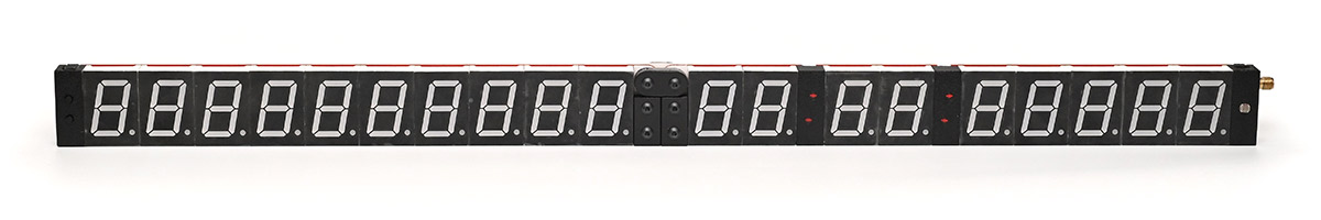
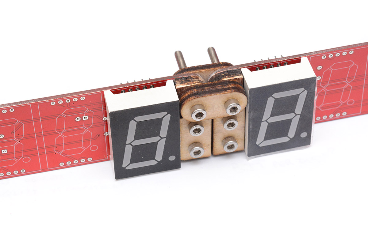
Another request I often had was to split the display onto two lines, as it's very wide otherwise. But some people love the very wide design, for the ISO timestamp aesthetic. There was only one way to please everyone: add an articulated joint, so the clock can transform from one to the other.
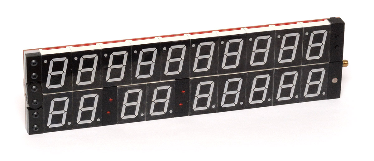
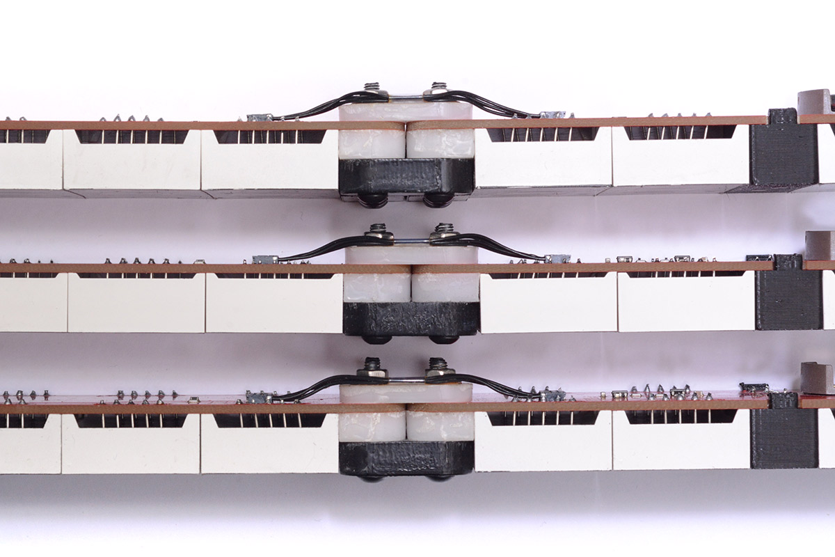
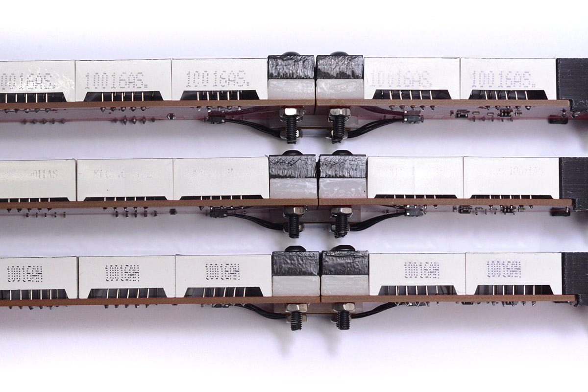
This substantially complicates the design of the clock, as we've now got multiple displays to keep in sync, and multiple processors to update. The connection across the hinge has to convey power, bidirectional data and ground, but also provide the analog signal for brightness level, and a latch signal to accurately control the display refresh. All of this is done over four wires. It also does firmware updates over the same four wires.
The hinge is made from laser-cut Delrin for maximum strength. The intention with this design was, in the wide configuration, that the shape of the hinge would subtly imply the letter T. It's not illuminated, but it goes some way towards our ISO8601 compliance.
One of the feature requests I had was to produce the precision clock as a clapperboard. This partly inspired the design of the Mark IV, although in the end I don't really recommend using it in this way, as the mechanical shock probably isn't good for it. It did mean that I chose a very secure coin-cell holder though. Clapperboard at your own risk!
Architecture
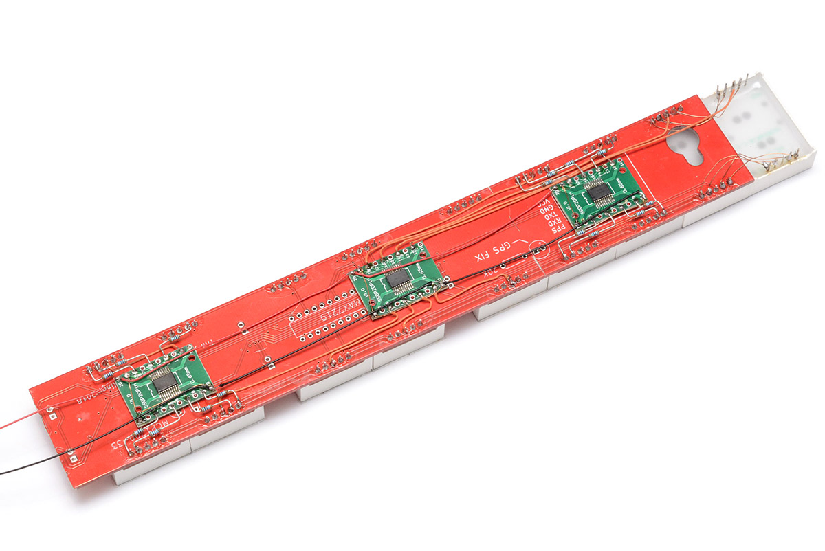
The previous clocks used off-the-shelf display drivers, which aren't an option as they have a fixed refresh rate of about 330Hz. Ideally we would drive every segment directly from a GPIO pin of a microcontroller, but with 19 digits (of 7 segments plus DP) that's 152 segments to control. We could use shift registers, it's certainly possible to latch them with high accuracy, but this was unappealing both because of the increased BOM cost (potentially one shift register per digit) and my aversion to high-speed signals in the design. A lot of clock customers are ham radio enthusiasts and care a lot about electrical interference. Multi-megahertz signals aren't necessarily bad, and certainly low-frequency signals are just as capable of causing interference if slew rates are not controlled, but I like to be able to tell people that there are no megahertz signals on board.
After a very long development period, I came up with the following system design, which uses two processors and six buffer chips.
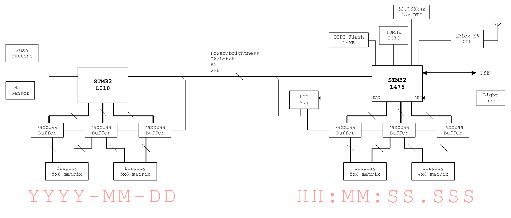
The display is split into four separate matrices, each arranged as 5 by 8. This lets us refresh the whole display in just five steps. It also means each matrix can be handled by a single 16-bit GPIO port. The idea was to set up the processors' DMA to drive the matrices in circular mode, so once configured, the display hardware has zero overhead. It means we can just place whatever data we want into an array, and it will get displayed for us. We can change the data in the array directly at any time. It even continues to work if we breakpoint the processor!
I spoke a bit more about the development of the display on this page about an automatic LED.
Display brightness is a huge problem, as it was solved so beautifully in the previous clock. With our DMA setup, we could also change brightness by PWM, just by making the array bigger and inserting dead time. But I didn't want to do that. It's essential that we maximise the duty cycle, or visibility under high-speed camera will suffer.
The buffer chips in the design solve the problem. The LEDs are voltage controlled. The main microcontroller is 3.3V logic. The matrix signals from the microcontroller are passed through the buffer chips, which are capable of operating at down to 1.8V, and we vary the voltage to the buffer chips to set the level of the matrix signals. This has a non-linear relationship with brightness, but that's fine, we can apply a non-linear curve in software.
In order to supply this varying power, I used an adjustable LDO and use the DAC output of the microcontroller to bend the feedback voltage. The display at full brightness will draw about 600mA, so this is the easiest way to provide that.
Only four wires pass across the hinge: power, ground, TX and RX. To save adding another wire, the brightness signal is transmitted by varying the power voltage. I specifically chose an STM32 chip that supported both 1.8V and 3.3V operation. In this way, we dim the voltage to the whole date side of the display, and it all works perfectly.
There's more cleverness to the hinge signals, as they need to show the display data at an exact moment in time. The conventional way of doing this is to provide a latch signal. Instead, I transmit UART data of what to display, and then a specific byte (a line ending) signals the receiving processor to disable its UART, and wait for the next falling edge on the wire (UART is idle high). At the instant we want to update the display, we send a single byte of 0xFE. The start bit of this byte triggers the update with sub-microsecond accuracy.
So we have power, bidirectional data, analog brightness control, and a high precision latch signal, all over four wires with the highest speed signal just 115200 baud.
Interface
Something I really enjoyed about the previous versions is that there was no interface. Nothing to configure, just power it on and it finds the time automatically. I definitely didn't want to compromise on that, in fact the auto-timezone means it's even better than before, but multiple display modes means we do need to have something.
Given that the update system mandates a USB port with mass storage device, we can easily add a config.txt file with as many parameters as we need. That's great for occasional tweaks to the clock behaviour, but really we want more than that. Eventually I settled on the following:
- There are a large number of clock display modes available, but most of them are turned off in the config file
- Buttons on the clock just cycle through the enabled modes.
In addition, later on I added a USB serial device, which can be used to send commands directly to the clock. I also implemented a hook, so that when the config.txt file is saved, the config is reloaded.
The double-buffered display
For the previous clock, which has its origins in the Mark II, I didn't really think about what I was doing. We get a PPS interrupt at the start of the second, and in the interrupt handling routine, I calculate what the display should show next.
This started off fairly reasonable, but it's a tricky situation. The serial data from the GPS module tells us what the time was at the preceding pulse. So when the next pulse comes in, we need to add one second to the time data we have. As the data had arrived in ASCII, and needed to be sent out in BCD, I ended up implementing the entire clock logic in BCD, in assembly. At one second to midnight on the 28th of February, there's a fair bit of calculation to do, and we need to do all of it in that few microseconds of the interrupt routine.
It gets worse as we added daylight saving time, and different timezones, and daylight saving time in different timezones. If you want to get a feel for how mad the final thing ended up, take a look at the source code for the mark III clock. All in assembly, all in BCD, all within the interrupt routine.
One of the "improvements" to the Mark IV clock is that the code is written in C, to make modification more accessible. I also wanted to manage the time sensibly. This means, when serial data arrives, we decode it into a unix timestamp. In preparation of the next pulse, we add one to it, and then we decode it into a string of local time using the standard C functions. Even with our faster processor, this does mean the whole thing takes a while, long enough to cause display jitter if we aren't careful.
The correct way to implement this is a double-buffer. If we imagine each second is deconstructed into a timeline, at about 0.5s we have received enough data from the GPS module to know what the time was at the last pulse. At 0.9s, we can start preparing the next display, which means we leisurely work out local time using the built-in C functions, and we put that data in a buffer (and send the date across the hinge). When the next pulse happens, all we need to do in the interrupt is swap the buffers (and send the latch signal to the date side). Even the most complex date calculations, like the dreaded ISO-week display, are now trivial to display with sub-microsecond jitter.
There is a complication to consider, with multiple display modes and a button to cycle through them. We might need to spontaneously change mode at any time. My solution is to check when the button press comes in whether we've already prepared the buffer, and if so, delay the mode switch until the next pulse. The effect is almost invisible, just that if you press a button when the display reads 0.9, there's a 100ms delay before it activates. Otherwise, the button presses are instant.
GPS discipline
One sore point, which has always been a pain, is that PPS is not guaranteed to happen each second. If the GPS fix is lost, the PPS signal stops. That means the "pulse" to swap the buffers could either be PPS, or our own timer rolling over. It gets especially confusing if we roll over, thinking that PPS is gone, but then moments later it arrives as we'd just happened to be running fast.
This was a big deal on the previous clocks, and the solution was to discipline the internal oscillator to the PPS signal. If PPS happened when our display was at 0.99, we make our oscillator a little faster. If it happened at 0.00, we slow it down and make sure not to accidentally roll over twice. There's also a chance of PPS appearing at some random offset, if we've lost it for a long time and it's suddenly come back, so that needs some extra care.
What I realised with the Mark IV is that disciplining our primary oscillator is completely pointless.
I want the clock to keep good time when it's lost signal, ideally within 1ppm, so that it takes 1000 seconds to drift 1 millisecond. To that end I fitted a reasonable quality temperature-compensated oscillator. There is no upper limit to how good an oscillator we could fit, but I chose something that seemed like a good compromise between cost and performance here. It's specifically 10MHz so that if the user feels like it, they can provide a better clock source. But even the one I fitted is vastly better than a normal AT-cut crystal (which themselves are better than the 32kHz quartz crystal you'd find in most clocks).
The TCXO is not driving a timer or interrupt, it's used directly as the external oscillator for the processor. The sinewave output of the part needed to be coupled to the oscillator-in pin via a small capacitor. I prototyped this by wiring it up to the L476-nucleo dev board. The LGA footprint needs to be mounted upside down and soldered with very fine wires.
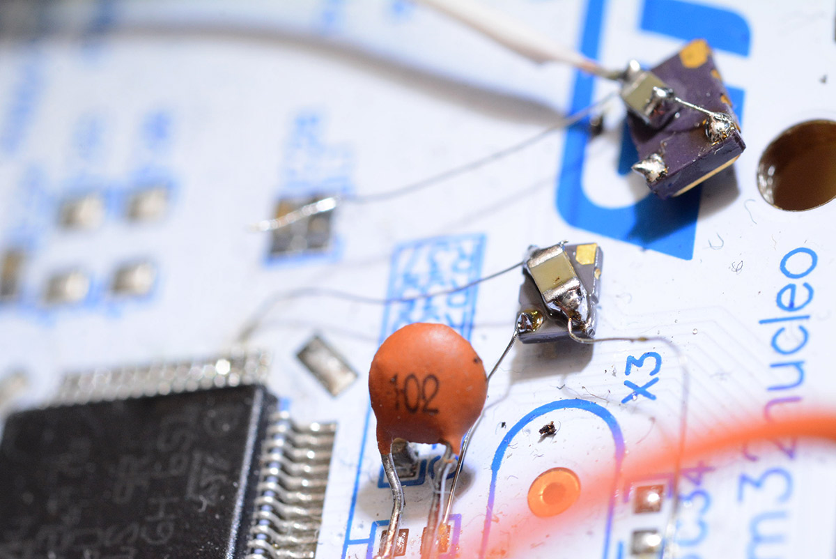
In the background is another model of TCXO which was also prototyped and rejected for some reason.
With the TCXO, I realised there is no point in disciplining it. A few PPM is such a tiny difference over one second, well beyond the capability of our display, that it's not worth the trouble. In the context of this clock, our primary time source is GPS, which gives us the long term stability. If we lose it, I'd rather we just explicitly show the degraded tolerance with the digits disappearing, than try to eek out a little bit more stability. Again, if the user has another time source available, such as a commercially made GPS-disciplined 10MHz oscillator, that's easy to connect up.
The main reason most clocks use tuning-fork style 32.768kHz oscillators is that they are substantially lower power than AT-cut crystals. One of the biggest complaints with the previous clock was the wait after turning it on: it can take a while to get a GPS fix. So this time, we fitted a coin cell battery so that immediately after turning it on the approximate time can be shown. The TXCO would drain power far too quickly, so we also added a (high quality) tuning fork oscillator.
You can get temperature compensated tuning fork crystals, but they're very expensive for what they are. The best type use a capacitor network to switch the load capacitance on the crystal as the temperature varies. Some of them can hold the time to within a couple of seconds a year. But given what we want it for, to keep approximate time while the clock is powered off, before reverting as quick as possible to the much better GPS time source, it didn't seem worth the added cost.
Additionally, I wasn't able to find a temperature compensated RTC module that allowed for subsecond precision. In contrast the onboard RTC of the STM32 does allow us to set the time to fractions of a second.
This time, it genuinely is worth disciplining the oscillator. We have PPS, so I set up a counter for the RTC crystal which monitors it over a few minutes and calculates the error. We're never going to get this perfect, as it will obviously drift with temperature, but we can get it much better than it would have been out of the box.
When the clock is first powered on, it takes note of how long it's been off. If it's less than a day, it sets the precision to 100ms. Otherwise, it turns off the fractional display entirely. It never drops the precision worse than one second, as at that point it's not particularly helpful, but if the clock shows no fractional second, it's clear that it's not synchronised in a long time.
The coin cell also gives the GPS module the ability to do a warm start, and it provides the processor with a small amount of battery-backed ram. This is used to hold the current timezone offset, and the daylight saving rules for the next decade, calculated from the database I'll explain in a moment.
The effect is that if you turn off the clock, and a daylight saving change happens while it's turned off, when you next switch it on it will show the correct time (to within the tolerance). In other words, the RTC "understands" daylight saving rules, even though it's actually just storing UTC.
(The one exception is if you turn off the clock, then carry it to a different timezone, and turn it on. Then it will need to get a full GPS fix before correcting itself, which I think is a fair requirement!)
Oscillator Oddness
Possibly the most interesting problem I encountered related to a subtle mistake on the PCB.
The PLL arrangements on STM32 are notoriously complex, and they provide an interactive flow diagram to help you set them up. I wanted the primary oscillator to be 10MHz, to maximise choices for people. But there's no specific PLL/prescaler arrangement that can get from 10MHz to 48MHz, needed to run the USB hardware. However, there is a way to jump from the low frequency 32.768kHz oscillator up to 48MHz. Perfect, we have it fitted, so let's use it, I thought.
The USB system worked fine, and the RTC worked fine. The DMA driven matrix displays worked fine. I had deliberately made the display matrix frequency adjustable: from 1000Hz to 100,000Hz, in case a specific frequency is needed, or some frequency caused interference problems, either with filming equipment or electrically. During testing, I used the USB port to set the frequency and it worked fine, except when I set the frequency to 30kHz.
At this point, the USB disconnected!
The astonishing problem was that one of the display signals was routed too close to the 32.768kHz quartz crystal, and when the display frequency was similar, it caused the crystal frequency to bend. Since the USB clock was derived from this crystal, it disconnected.
The fix, once I'd figured it out, was dead simple, just keep those display signals well away from the sensitive crystal. But if I hadn't fed the USB clock from here, I may never have noticed the problem. This little bodge wire fixed the prototype, but on subsequent PCBs I simply used a different pin for that signal.
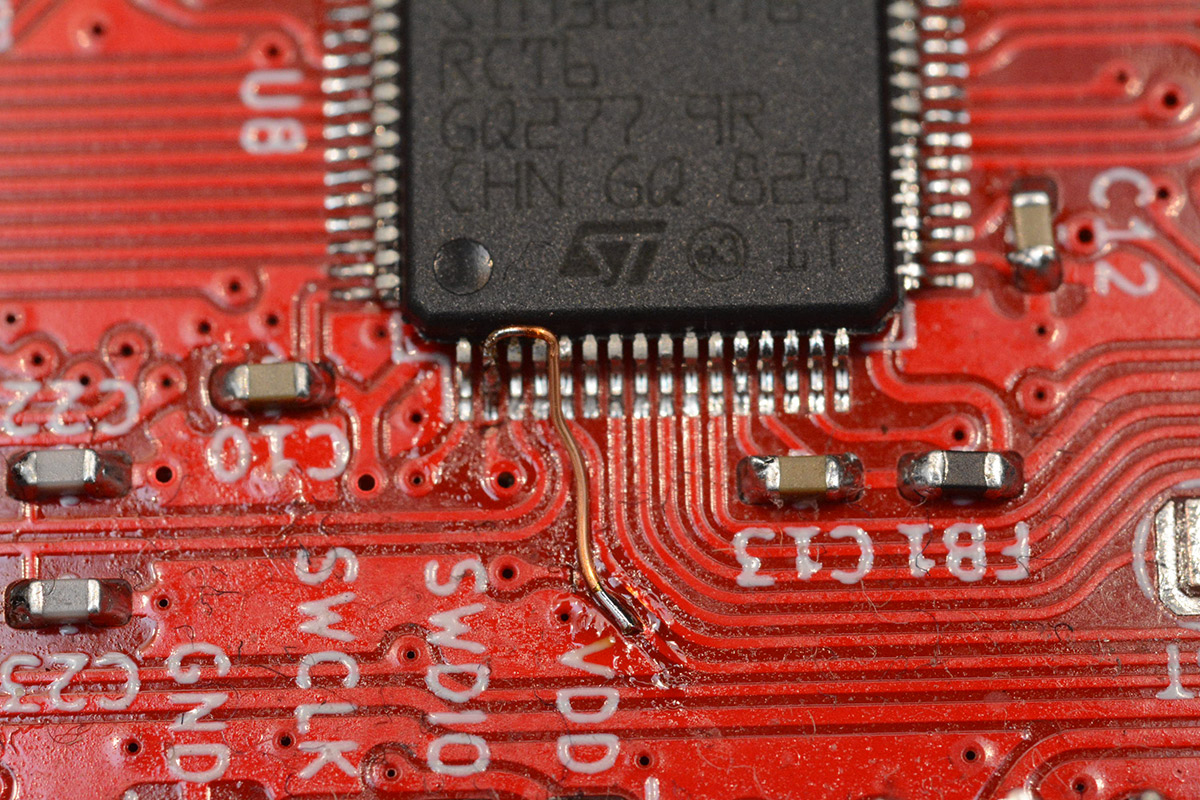
The advice for routing tracks to crystals is to keep them as short as possible, and in the design above you can see how embarrassingly far away I'd located it (just out of sight to the left). The processor has an amplifier that boosts the tiny signal from the crystal. In this specific arrangement, because of the physical size of the processor and the position of the through-hole pins for the digits, placing it directly adjacent wasn't an option. I was able to shuffle things around and get it a tiny bit closer on the next revision, but the main repair was just to not route anything else near it.
Interrupt vector hot-swap
The interrupt vectors are like a list of function pointers, pointing to functions that will run when the interrupts happen. The "Nested Vectored Interrupt Controller" (NVIC) of ARM chips is a bit of a step up from the simple AVR interrupt system, with the possibility of interrupting your interrupts, but fundamentally it's the same idea. We want our PPS (external interrupt) function to run with the lowest possible latency, and the SysTick interrupt, configured for 1kHz, will update the milliseconds of the display. Although this is double-buffered, the actual task to be performed is going to depend on which mode the clock is in, and what the current precision should be. With count-up, count-down, "other", and three levels of precision, we're potentially facing a stack of conditional branches within the interrupt, and branches on STM32 mean stall cycles.
A much more elegant way to do it is to move the interrupt vectors to RAM, and dynamically swap the function pointers depending on mode and precision level. This is a common and expected technique, but doing it in C in a way that's not horrifically ugly takes a fair bit of thought. Moving the vectors is as simple as copying them to the new location and writing to the relevant register, like this:
memcpy((void*)0x20000000, (void const*)0x08000000, 0x188); SCB->VTOR = 0x20000000;and then re-assigning the SysTick interrupt could, I suppose, be done like this:
#define SetSysTick(x) *((uint32_t *)0x2000003C) = (uint32_t)xPreprocessor macros can always be used to make it explicit what we're doing, but in my attempt to keep the code somewhat sane, I tried to do this "properly". I first altered the linker script to declare the first 392 bytes of RAM as a separate section:
MEMORY { VECT (xrw) : ORIGIN = 0x20000000, LENGTH = 392 RAM (xrw) : ORIGIN = 0x20000188, LENGTH = 96K - 392 ...then within the sections, we declare a couple of symbols, which we'll later reference:
.isr_vector : { . = ALIGN(4); __VECTORS_FLASH = .; KEEP(*(.isr_vector)) /* Startup code */ . = ALIGN(4); } >FLASH .isr_vectors_ram : { __VECTORS_RAM = .; } >VECTNow within our C code, we can declare these as external uint32 arrays.
extern uint32_t __VECTORS_FLASH[]; extern uint32_t __VECTORS_RAM[];Our startup code now actually makes sense:
memcpy(__VECTORS_RAM, __VECTORS_FLASH, 0x188); SCB->VTOR = (uint32_t)&__VECTORS_RAM;and reassigning SysTick now almost doesn't even need the macro:
#define SetSysTick(x) __VECTORS_RAM[15] = (uint32_t)xThe arcane syntax of linker scripts is something I've always struggled with, so coming up with something that's almost elegant still feels like a win. It possibly wasn't necessary, but forcing ourselves to figure this out is the only way to learn. And the linker scripts will need plenty of further wrangling when it comes to the bootloader...
The chain-loading bootloader
One of the most important things with this clock is that updating the firmware is easy. I have made a big deal about this in the past, of how shameful it is to ask your users to install a driver. I wanted to do it right.
I designed this clock before the Raspberry Pi Pico came out. The RP2040 wouldn't have been sufficient to run the clock as it has no hardware FPU (the successor, the RP2350 would be fine). But these chips allow updates through a mechanism known as UF2. If I had known about it, I would have used it. Instead I created something very similar, and functionally the same from the user perspective.
In addition to updating the firmware, we want to be able to update the timezone database and the shapefiles for the world maps. This adds up to about 12MB of data, so I kitted out the clock with a 16MB flash memory chip. I considered fitting an SD card, which at least has a fool-proof method of updating, but it's increasingly difficult to find small size SD cards and dealing with exFAT adds some overhead I'm not interested in.
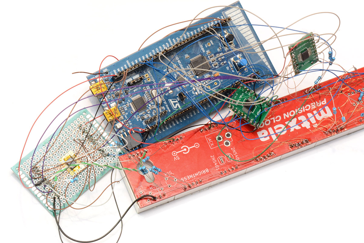
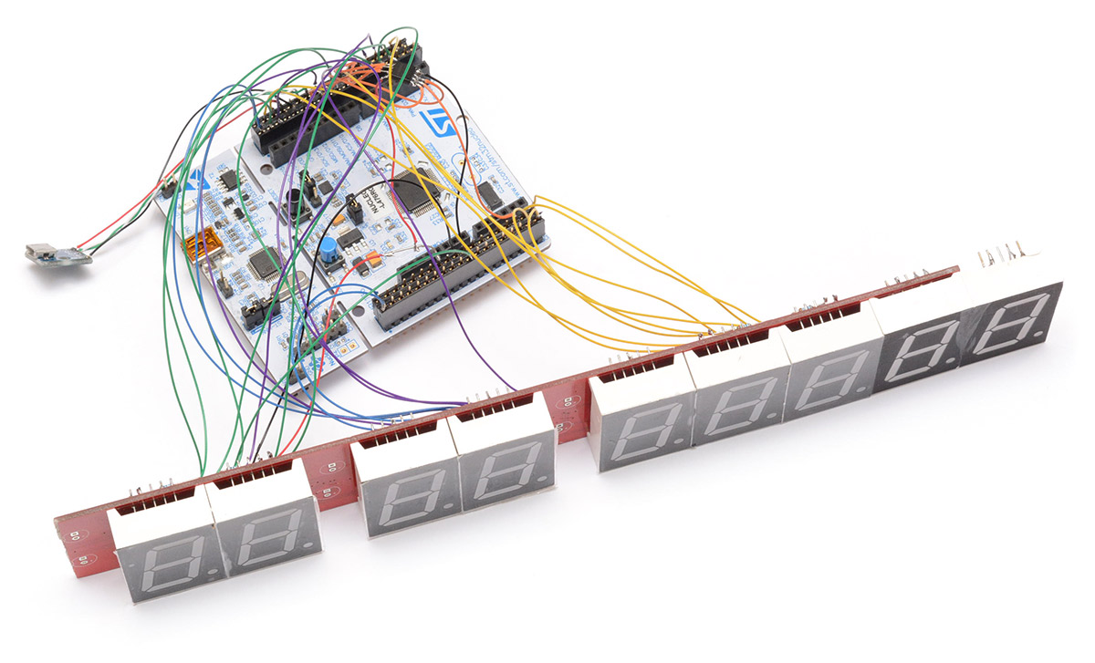
So the design was to have the USB port present a small mass storage device. We can just copy and paste the necessary files onto the drive, and no drivers are needed. My dev board at this point looked like this:
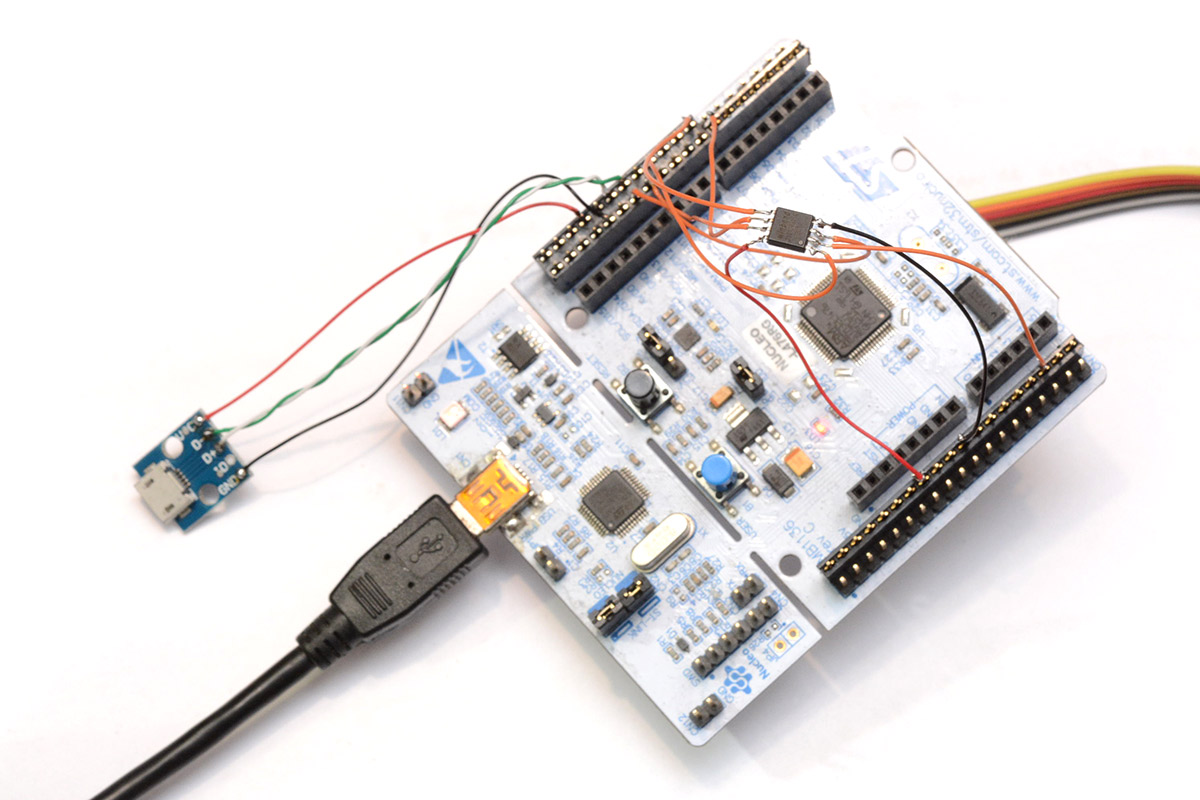
The foremost consideration is that we never end up in an unrecoverable state. An ST-link SWD header is the ultimate backup but we can't expect the user to have the programming cable. STM32 chips come with a system bootloader, a piece of ROM that runs a few basic protocols, and one of them is DFU over USB. We can trigger this bootloader using the dedicated pin for it. But USB DFU requires a driver on the host side; I'm not interested in using it. I took the boot pin out to a small pad, as a secondary line of defence, if absolutely necessary the user could short this pad, trigger the DFU update using a driver.
For the main bootloader, we present ourselves as a mass storage device. The first thing we do on power-up is verify the currently loaded firmware by checking the CRC. If it's wrong (either because of a failed update, or it's blank) then we definitely don't want to launch the main application. Next we check the flash memory, and if it finds a firmware image on there, and the CRC is correct, and it's a different firmware to what's currently loaded, then we can perform an update. The USB stack is not triggered until it has decided what to do. Only in the case of no valid firmware being available does the bootloader's mass storage device enumerate, where it then hangs waiting for you to copy a valid image across.
Otherwise, it launches the main application. This has its own USB stack which I eventually configured as a composite device, both a mass storage device and a serial port for controlling the clock.
The first thing the application does is query the second microcontroller over the hinge connection. That microcontroller responds with its own firmware CRC. If there's a new firmware image on the flash memory, we can now chain-load the update across the hinge. Instead of using a custom bootloader on the second microcontroller, I made use of the more reliable system bootloader. I specifically used the same UART pins for the hinge connection as the system loader uses, and on the application side of the main processor I re-implemented the entirety of the STM32 bootloader protocol. The UART sends a command to trigger the system loader, the update is performed (while showing a cool progress animation) and then the secondary microcontroller launches its application.
One concern I always have with this stuff is whether a sudden power cut could cause problems. We have a full backup of the firmware image on the flash memory, so it should be possible to recover from a power cut gracefully. The one situation I had to make a call on was whether to add a dedicated signal for the second microcontroller's BOOT0 pin. If we cut the power at exactly the right moment, it may end up with a partial firmware image that runs but doesn't respond to the command to re-enter the system bootloader. If we had hardware control of the power and the BOOT0 pin from the main microcontroller, we could recover, but that means adding more wires to the hinge, wires which are redundant except for this exact scenario. I decided to risk it. If ever a power cut does happen at that exact moment, the user can short the BOOT pad manually on the back of the clock to recover.
I did consider having the secondary microcontroller always boot into the system loader, but there are a few annoyances with doing so, and powering up the clock would be much more clunky.
I probably spent more time on the chain-loading bootloader than on any other aspect of the clock. The end result is a work of art, even if it's one that nobody else will appreciate. I spent a long time monitoring the SCSI commands sent by the host OS during different operations and on different systems. Windows, linux and OSX all have slightly different behaviour when, for instance, you "eject" a mass storage device (which is different to just unmounting it). Unlike the Pico, which immediately disconnects and performs the update when the file is copied, I wait before performing the update, as there may be several files you want to copy across, two firmware images, the database and the map file. Once copied, we could just power-cycle the clock, but it's more swish to "eject" the device, which then performs the updates with its cool animations, and reconnects when it's ready.
The external flash memory has pages of 4kB. If you want to write to it, you need to erase an entire page, and write it back. I chose FAT12 or FAT16 as the filesystem, as they're widely supported and quite simple. FAT12 may seem like an odd choice but it's so old that it makes efficient use of the storage available, if that's a concern. The USB mass storage class is really a wrapper for SCSI commands, which was a bit of a surprise to me. While we have FATFS running on the clock, for interpreting the files, that's totally independent to the mass storage USB device, which essentially just provides "read" and "write" access to the host.
This presents a bit of a problem as to do this properly we would need to accept arbitrary writes, store them in RAM, then erase a whole page and write it again. This feels inherently dumb as the flash memory has a limited number of write cycles, so if we copied 4kB in small chunks, it would erase and re-write the page repeatedly. I suppose we should have made a proper cache system, with several pages in RAM that then get written asynchronously, but the write process is slow. My simple solution to all this was to set the block size of the file system to 4K. This is a bit of a gamble as it's extremely unusual to have a block size other than 512, but I've tested it with Windows, Linux and OSX without problems. By setting the block size to 4K, we essentially force the changes to the filesystem to be a page at a time.
I don't expect the memory to be written to that often, it's only every few months that the database changes. There are wear-levelling filesystems available but they're quite a bit more complex. I chose a QSPI flash memory chip that's rated for at least 100,000 writes, but my ultimate cop-out is that it's in a SOIC-8 footprint, so it's one of the easiest surface mount parts to replace.
Auto timezone
Possibly the most requested feature, automatically setting the timezone based on the GPS coordinates was essential. However, most people don't realise how complex this process is, at least within the restrictions I'd given myself: no internet or cellular modem, nothing beyond the GPS data, and a USB port for occasional updates.
If we had an internet connection, sure, we could just query an online service. But I don't want my clock to require wifi.
If we had a cellular modem, we could get the time from the cell towers, which is broadcast through a protocol called NITZ. This is how phones auto-update when you enter a different timezone, but it's somewhat unreliable depending on the carrier, and overall worse than using GPS. And I really don't want my clock to have a sim card.
I'd also like, just for the sake of it, for the clock to work anywhere in the world, even at sea.
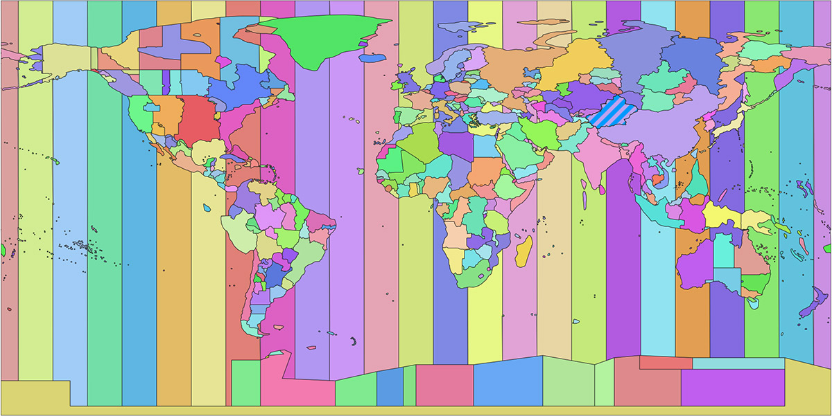
This means we need to keep a copy of the map data for the country outlines for the whole world. It also means we need a full copy of the timezone database, and have the processing power onboard to make use of all this.
We can break it down into two parts, first of all is determining the IANA timezone name from GPS coordinates. This is a solved problem, at least on desktop computers. A project called Timezone Boundary Builder has collated this data, extracted from OpenStreetMap. There are moderately frequent updates to it, which is fine.
Another project, ZoneDetect, is an example of how to use this data, written in C. In theory, all we need to do is port ZoneDetect to a microcontroller.
It ended up being a fair bit of work, because ZoneDetect was written for desktop computers with infinite RAM. The shapefile is about 11MB, which doesn't sound like much, but the first thing ZoneDetect does is mmap() the whole thing into memory. The STM32L476 running the show only has 128kB of RAM.
The shapefile on the external flash memory is accessed repeatedly as it searches through the file. We're using FATFS, by our hero ELM ChaN, to read the filesystem. The QSPI reads have to be carefully locked in case of any USB activity (in fact, if any USB read or writes to the flash memory are detected, we abort any ongoing zone detection for the next few seconds). When I finally got the program running on the chip, it was a great relief, but it took several seconds to figure out my coordinates mapped to Europe/London. This is on the 80MHz ARM Cortex M4 with FPU.
It's possible we could reconfigure the shapefile to minimise the number of random accesses. I ended up plotting some graphs of which addresses are accessed, and some clear patterns emerged. The two main activities were searching forwards, and searching backwards, so I split these into separate calls. Each one loads data from the file, and also caches the page ahead (or behind). Experimentally, caching about half a kilobyte ahead seemed to give the best performance. I got the behaviour down to about 500ms in most cases, which I considered good enough.
Once we've managed that, we need to load the database rules for that location. I'm repeating myself here, but I'll say it again, there is no central authority on timezones. Every government makes up whatever it likes. "The Timezone Database", the Olsen tzdb, is just a guide, an approximation assembled as a best guess. It's an incredible project, but it comes with disclaimers about accuracy, and it's immensely complex. There are over 500 timezone entries, and the database is updated multiple times a year.
The database is surprisingly readable, and is intended primarily for human consumption. You tend to have several paragraphs of prose, followed by one line of data. I heartily recommend giving it a read, it's fascinating. For a while I was subscribed to the timezone database mailing list. A lot of people have very strong opinions about timezones, particularly how the historical data is presented (which is very important in some situations, thankfully not for us).
If we take a look at the europe file, and search for Europe/London, after pages of comments we get to the actual data:
# Zone NAME STDOFF RULES FORMAT [UNTIL] Zone Europe/London -0:01:15 - LMT 1847 Dec 1 0:00 GB-Eire %s 1968 Oct 27 1:00 - BST 1971 Oct 31 2:00u 0:00 GB-Eire %s 1996 0:00 EU GMT/BSTOnly the last line matters, which says since 1996 we've had the standard offset of 0:00 from UTC, and follow the daylight saving rules known as EU.
Searching for Rules EU, we find the following:
# Rule NAME FROM TO - IN ON AT SAVE LETTER/S Rule EU 1977 1980 - Apr Sun>=1 1:00u 1:00 S Rule EU 1977 only - Sep lastSun 1:00u 0 - Rule EU 1978 only - Oct 1 1:00u 0 - Rule EU 1979 1995 - Sep lastSun 1:00u 0 - Rule EU 1981 max - Mar lastSun 1:00u 1:00 S Rule EU 1996 max - Oct lastSun 1:00u 0 -To "max" means the last two lines are still valid, and that we start DST from 1AM UTC on the last Sunday of March, and end DST at 1AM UTC on the last Sunday of October. This is one of the simpler rules in the database, after all, Europe switches DST all at the same time, whereas in the US the switchover is at 2AM local time.
Attempting to parse the database on the fly, that is, asking if today is the last Sunday of the month every time the seconds interrupt fires, is not viable. Even for desktop computers the database is preprocessed into a more easily parsed format. The tz database also includes some reference implementations of how to use it, but once again these are aimed at desktop computers and servers.
For the previous clock, I managed to solve this problem by pre-calculating all of the dates where changes occur, for the next hundred years. A simple javascript utility spat them out and a compile-time definition included the relevant lines. In that case, I just checked whether the month was March/October and the day was the recorded number. It got more complex for some of the zones, like New Zealand, where the switch happens on the first Sunday of April, because that can occasionally land on the first of the month. In that scenario, the UTC month will be different to the local month, because they're 12 hours ahead.
But fundamentally, I became convinced that precalculating the switchovers was the most sensible option. The tz db includes a utility called zdump. If passed the right arguments, we can get it to tell us the switchover times for any zone, for any range of years.
$ zdump -V Europe/London -c 2020,2030 Europe/London Sun Mar 29 00:59:59 2020 UT = Sun Mar 29 00:59:59 2020 GMT isdst=0 gmtoff=0 Europe/London Sun Mar 29 01:00:00 2020 UT = Sun Mar 29 02:00:00 2020 BST isdst=1 gmtoff=3600 Europe/London Sun Oct 25 00:59:59 2020 UT = Sun Oct 25 01:59:59 2020 BST isdst=1 gmtoff=3600 Europe/London Sun Oct 25 01:00:00 2020 UT = Sun Oct 25 01:00:00 2020 GMT isdst=0 gmtoff=0 Europe/London Sun Mar 28 00:59:59 2021 UT = Sun Mar 28 00:59:59 2021 GMT isdst=0 gmtoff=0 Europe/London Sun Mar 28 01:00:00 2021 UT = Sun Mar 28 02:00:00 2021 BST isdst=1 gmtoff=3600 Europe/London Sun Oct 31 00:59:59 2021 UT = Sun Oct 31 01:59:59 2021 BST isdst=1 gmtoff=3600 Europe/London Sun Oct 31 01:00:00 2021 UT = Sun Oct 31 01:00:00 2021 GMT isdst=0 gmtoff=0 Europe/London Sun Mar 27 00:59:59 2022 UT = Sun Mar 27 00:59:59 2022 GMT isdst=0 gmtoff=0 Europe/London Sun Mar 27 01:00:00 2022 UT = Sun Mar 27 02:00:00 2022 BST isdst=1 gmtoff=3600 Europe/London Sun Oct 30 00:59:59 2022 UT = Sun Oct 30 01:59:59 2022 BST isdst=1 gmtoff=3600 Europe/London Sun Oct 30 01:00:00 2022 UT = Sun Oct 30 01:00:00 2022 GMT isdst=0 gmtoff=0 Europe/London Sun Mar 26 00:59:59 2023 UT = Sun Mar 26 00:59:59 2023 GMT isdst=0 gmtoff=0 Europe/London Sun Mar 26 01:00:00 2023 UT = Sun Mar 26 02:00:00 2023 BST isdst=1 gmtoff=3600 Europe/London Sun Oct 29 00:59:59 2023 UT = Sun Oct 29 01:59:59 2023 BST isdst=1 gmtoff=3600 Europe/London Sun Oct 29 01:00:00 2023 UT = Sun Oct 29 01:00:00 2023 GMT isdst=0 gmtoff=0 Europe/London Sun Mar 31 00:59:59 2024 UT = Sun Mar 31 00:59:59 2024 GMT isdst=0 gmtoff=0 Europe/London Sun Mar 31 01:00:00 2024 UT = Sun Mar 31 02:00:00 2024 BST isdst=1 gmtoff=3600 Europe/London Sun Oct 27 00:59:59 2024 UT = Sun Oct 27 01:59:59 2024 BST isdst=1 gmtoff=3600 Europe/London Sun Oct 27 01:00:00 2024 UT = Sun Oct 27 01:00:00 2024 GMT isdst=0 gmtoff=0 Europe/London Sun Mar 30 00:59:59 2025 UT = Sun Mar 30 00:59:59 2025 GMT isdst=0 gmtoff=0 Europe/London Sun Mar 30 01:00:00 2025 UT = Sun Mar 30 02:00:00 2025 BST isdst=1 gmtoff=3600 Europe/London Sun Oct 26 00:59:59 2025 UT = Sun Oct 26 01:59:59 2025 BST isdst=1 gmtoff=3600 Europe/London Sun Oct 26 01:00:00 2025 UT = Sun Oct 26 01:00:00 2025 GMT isdst=0 gmtoff=0 Europe/London Sun Mar 29 00:59:59 2026 UT = Sun Mar 29 00:59:59 2026 GMT isdst=0 gmtoff=0 Europe/London Sun Mar 29 01:00:00 2026 UT = Sun Mar 29 02:00:00 2026 BST isdst=1 gmtoff=3600 Europe/London Sun Oct 25 00:59:59 2026 UT = Sun Oct 25 01:59:59 2026 BST isdst=1 gmtoff=3600 Europe/London Sun Oct 25 01:00:00 2026 UT = Sun Oct 25 01:00:00 2026 GMT isdst=0 gmtoff=0 Europe/London Sun Mar 28 00:59:59 2027 UT = Sun Mar 28 00:59:59 2027 GMT isdst=0 gmtoff=0 Europe/London Sun Mar 28 01:00:00 2027 UT = Sun Mar 28 02:00:00 2027 BST isdst=1 gmtoff=3600 Europe/London Sun Oct 31 00:59:59 2027 UT = Sun Oct 31 01:59:59 2027 BST isdst=1 gmtoff=3600 Europe/London Sun Oct 31 01:00:00 2027 UT = Sun Oct 31 01:00:00 2027 GMT isdst=0 gmtoff=0 Europe/London Sun Mar 26 00:59:59 2028 UT = Sun Mar 26 00:59:59 2028 GMT isdst=0 gmtoff=0 Europe/London Sun Mar 26 01:00:00 2028 UT = Sun Mar 26 02:00:00 2028 BST isdst=1 gmtoff=3600 Europe/London Sun Oct 29 00:59:59 2028 UT = Sun Oct 29 01:59:59 2028 BST isdst=1 gmtoff=3600 Europe/London Sun Oct 29 01:00:00 2028 UT = Sun Oct 29 01:00:00 2028 GMT isdst=0 gmtoff=0 Europe/London Sun Mar 25 00:59:59 2029 UT = Sun Mar 25 00:59:59 2029 GMT isdst=0 gmtoff=0 Europe/London Sun Mar 25 01:00:00 2029 UT = Sun Mar 25 02:00:00 2029 BST isdst=1 gmtoff=3600 Europe/London Sun Oct 28 00:59:59 2029 UT = Sun Oct 28 01:59:59 2029 BST isdst=1 gmtoff=3600 Europe/London Sun Oct 28 01:00:00 2029 UT = Sun Oct 28 01:00:00 2029 GMT isdst=0 gmtoff=0It extrapolates out into the future as far as you'd care to go, and obviously it's questionable how much we can say about daylight saving rules hundreds of years in the future, but this is an output I can work with. A python script was used to run through every zone, and inhale the DST rules until the year 2106, interpreting each transition time as a Unix timestamp and an offset (the archaic gmtoff in the lines above).
I chose 2106 as a cutoff because that's the 32bit rollover of the Unix timestamp. Everyone's heard of the 2038 problem, but that's an overflow of a signed 32 bit number. Unsigned, we can delay the problem until 2106! But seriously, the GPS data only has a 2-digit year, so in the event the clock is still going by the year 2100, we'll need a firmware update anyway.
The compressed data, along with a lookup mechanism that made some amount of sense, ended up at about 175kB. With that, we finally reached the point where the clock can figure out the exact local time, from nothing but GPS.
I've glossed over a lot of stuff in this summary, but implementing all of this took forever, maybe several months of solid work. Phew!
Interrupt priorities
We heard you like interrupts, so we stuck pre-emption priorities in your NVIC so you can interrupt while you interrupt, or something.
The possibility of using an RTOS to run the clock was dismissed fairly quickly, because I didn't believe it would be sufficiently real-time. The prime directive is to make the clock display infallible and the only way to achieve that is by going bare metal. Given the number of tasks that need completing at specific moments in the timeline I ended up writing something that approaches the complexity of an RTOS anyway, but it's all handled through the interrupt controller.
This is something of a minefield because as soon as we start fiddling with the priorities the HAL functions can have weird problems and edge cases. Most functions expect to be pre-empted by SysTick, and rely on it for timeouts when problems occur. If you call a HAL function from within SysTick, or something higher priority than it, then it will still work, right up until it doesn't work, never times out and effectively hangs the processor.
At the very top, our two most important tasks are servicing PPS, and the SysTick interrupt that updates the milliseconds of the display. Early versions of the clock would have the display flicker slightly when files were copied to the USB drive, which I considered unacceptable. With the lower priority for USB interrupts, transactions take longer but the display remains stable.
At the other end, the lowest priority and slowest task is doing our ZoneDetect. Since this can take a good fraction of a second, we stick this in the main loop. It is basically the only thing that happens there, along with a few "delayed" tasks that get requested by certain flags, everything else is done in an interrupt context.
A really neat feature of the UART hardware on the L476 is the ability to do a character-match interrupt. We can receive NMEA data from the GPS module into a buffer via DMA, and just get an interrupt when a line-ending is detected. This is super efficient and I wish all microcontrollers had something like this. Incidentally, unlike the previous versions of the clock, we do actually check the checksums of the NMEA strings and discard them if necessary.
So we have high, medium and low priorities, plus the base level of the main loop outside of the interrupt context. But beyond that, we ideally need to jump to different levels of priority at certain tasks. When PPS happens, we immediately want to activate the timing-critical code to get the best possible latency regardless of what else is happening. But we also want to do a bunch of other stuff that is not quite so important and may rely on HAL timeouts and so on. For this, we can trigger a software interrupt (in this case, PendSV) that runs at a lower priority, triggered at the end of PPS or seconds rollover.
There's a lot of asynchronous stuff that happens and in some ways it's a mess, but it's a mess that works with extremely low latency. The thing to watch out for is that a lot of C code is not "thread safe" meaning that interrupted operations can potentially have data corrupted. A classic example is bitfields in structs, which are accessed through multiple opcodes that depend on register state that is not preserved by the interrupt controller. This feels like a complete failing of the compiler, as it results in code that works most of the time but occasionally doesn't. My only solution is to avoid bitfields entirely.
That's a complaint about GCC, but I have many more complaints about STM32CubeIDE. I've ranted in the past about how awful the UI is, the unbelievable failures in its crushed java interface. They recently somehow made the IDE even worse, by forcing you to "log in" to use it, and yet they still haven't fixed the most basic glitches that make it torturous to use, glitches that I complained about five years ago when I started this project and that still exist today.
Perhaps the most offensive UI problem is that if you change the build mode from "Debug" to "Release" and then click "run code", it will compile the Release version, and then flash the Debug version. This can be almost impossible to notice unless you're doing something weird enough that the optimisations break it. An example is jumping to the main application from the bootloader. All I want to do is generate a jump instruction, but it's incredibly painful to do that in plain C. With linker script wrangling much like the vector table shifting I described above, I was able to reduce the jump to something like this:
__set_MSP(_app_start[0]); ((void (*)(void)) _app_start[1])();The first entry in the vector table is stack pointer, the second entry in the vector table is the application entry point.
This worked nicely, and I considered the bootloader finished. When I started flashing boards via the ST-link utility, however, they didn't work! Outside of the IDE, which I thought had been running the "release" build, the code hadn't actually been tested with optimisations enabled. A failure at this point in the bootloader is catastrophic. The fix is trivial (just disable optimisations for those lines of code) but I was incredulous that the problem had gone unseen at all.
Display design
The big question was how the display was going to work, and I've lost track of the number of different options I considered. I really wanted to reuse the analog current-mirror display brightness idea, and for a while I was yearning for a parallel-input LED driver chip, the kind of thing that used to exist in the 90s but no one makes them now. It would have allowed me to use the reference current to set the brightness, but kept all the options open for how to drive things. The idea of driving the display with discrete transistors was on the table for some time. I considered LED driver shift registers, which are shift registers with a reference current input, which would have worked but have their own downsides. For one, we'd need a lot of them, to drive our ~150 segments, which would make the PCB layout difficult and the BOM cost increase significantly (regular shift registers are very cheap, but the LED driver chips with settable current are pricey). As current sinks, they'd need to be driving common-anode displays, whereas the previous clock used the more widely available common-cathode. Finally, mirroring the current to 10 or 20 shift registers is nontrivial, it would either require a lot of extra transistors or something hacky.
I'm not saying the final design is not hacky, but it meets the spec and only requires six reasonably cheap buffer chips. We split the display into four separate matrices, as a compromise between direct drive and a full matrix. We control each matrix directly from microcontroller GPIO, via DMA. The LEDs are voltage-controlled, and we use buffer chips on the output signals as a means to control the brightness. They each function as a kind of analog, continuously variable level shifter, that also boosts the maximum current we can deliver.
As an illustration, imagine driving a four-by-four LED matrix this way:
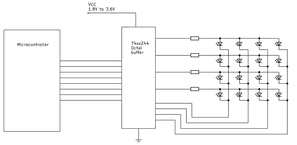
The buffer chip needs to sink and source current. We also need some amount of current limiting, although how much is not clear. It provides some protection against burning out if the matrix stalls, and it goes some way to evening out the current between LEDs, which may not have perfectly matched bandgaps. Too large a resistance will limit our maximum brightness, however.
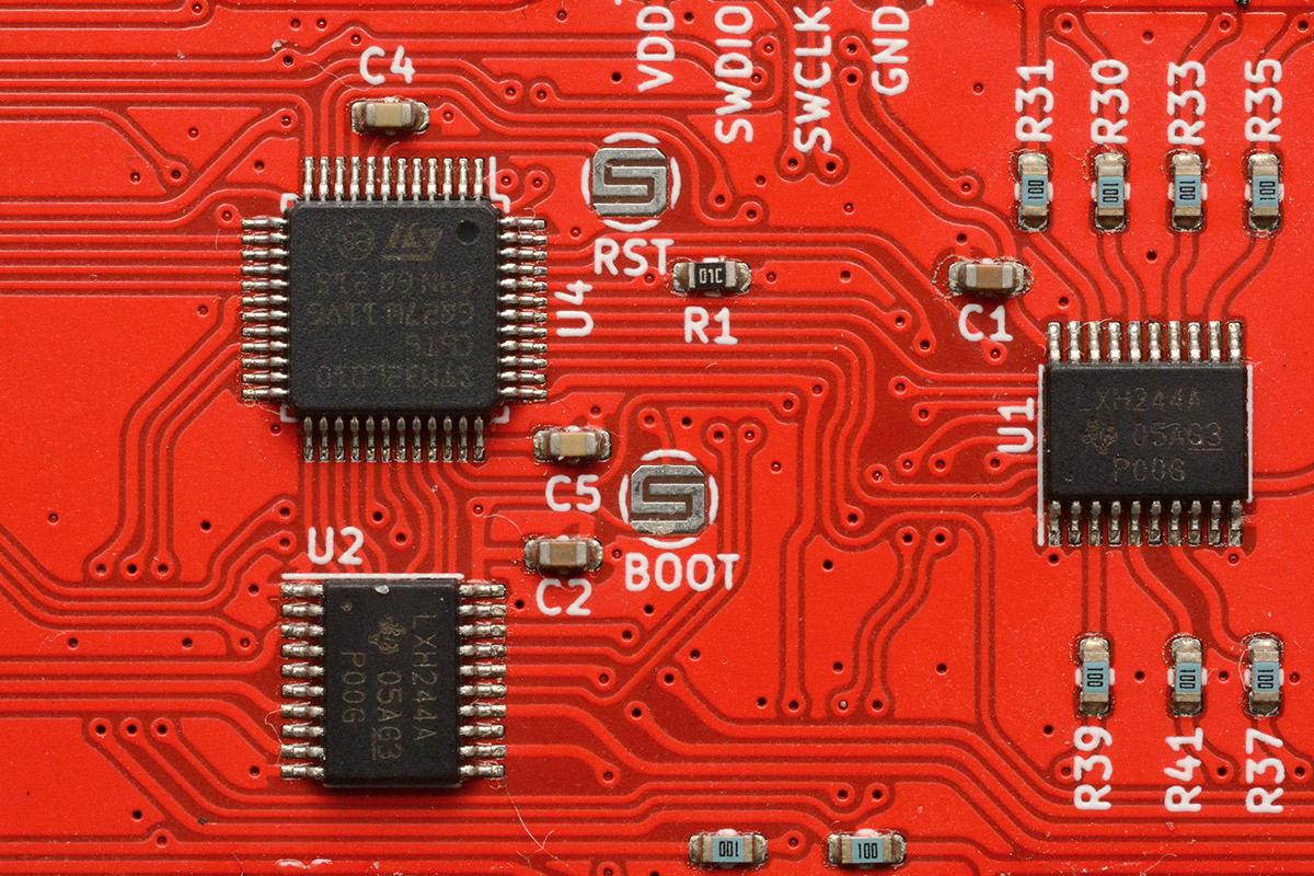
There's a whole range of 74 series octal buffer chips that end with 244, where the prefix and the letters in the middle tell us about their performance and characteristics. Of concern are the supply voltage range, the output current capability, the switching speed, and I suppose the cost. Happily, they mostly have the same footprints, so we can defer the decision until later.
Our matrix needs to refresh at around 100kHz, which means a switching speed of 500kHz, if there are five digits per matrix. We then set the display brightness by dipping the power supply to the buffer chip. I wasn't sure this was going to work until I prototyped it, which I began by tediously wiring up the SSOP20 buffer chips with magnet wire.
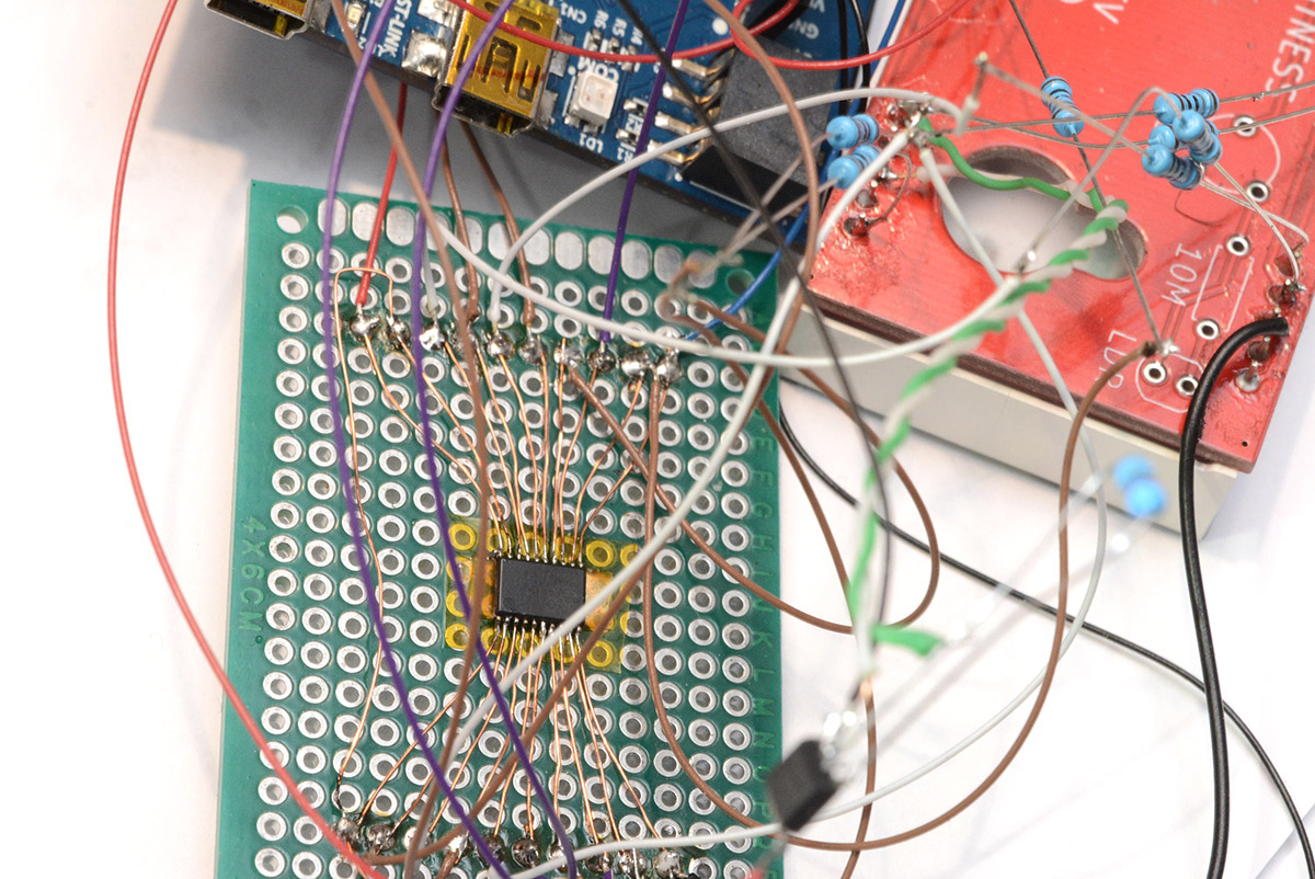
This quickly grew tiresome so I ordered some breakout boards. I took one of the old clock PCBs, cut the lines to the cathodes, and wired our new display circuit idea up to it.
The blue devboard is for an STM32F072, which I originally planned to use for the date side of the clock.
The results were promising, so to wire up the time-side, I tried to make things a little tidier.
Visible in the picture above is the knife-cut I made to the existing matrix wiring on the PCB, to split it into two matrices. The final four digits make up the last matrix, with the last digit super-glued in place and the matrix extended manually. Thus the time-side prototype came together, and on this I developed the bulk of the firmware.
I don't remember all of the part numbers used, but the final choice of buffer chip was SN74LVTH244A, and the limiting resistors were 10ohm. Technically this buffer chip has a minimum voltage of 2.7V, but it functions correctly down to 1.8V, and has good current and switching characteristics otherwise. A backup plan, had I not been able to reach the desired output current, was to stack the buffer chips. This is an old technique that probably doesn't translate too well to surface mount, but you just solder another chip directly on top, and it doubles the output current.
In the end I probably could have eliminated the current limiting resistors entirely, as the DMA matrices continue to cycle even when the processor hangs, but it's best to have them on the PCB, and if not needed we could replace them with 0-ohm resistors.
Brightness details
Until the first PCB, I was dipping the buffer chip voltage manually from the bench power supply. Perhaps there's a suitable way to wire up a light sensor directly to a variable power supply, but given the response of the LEDs, I fully expected to have to control this digitally. The light sensor goes into the main processor's ADC, a non-linear curve is applied, and a DAC output then controls the brightness.
One could simply send the DAC value through a beefy op-amp with enough current output, but that'd be expensive and we don't exactly need the bandwidth. A simpler option is to take an adjustable voltage regulator, and control it by bending the feedback voltage. These adjustable regulators simply expose the feedback pin, with the intention that you feed it from a potential divider on the output. There'll be some internal voltage reference, maybe 1.2V, and the regulator will do what it can so that the feedback pin meets that voltage. The datasheet for the TPS784 adjustable LDO has this diagram:
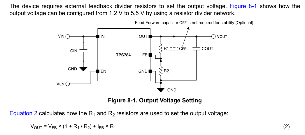
What we want to do is add a third resistor into that network, driven from the DAC, so that the full range of DAC output (0.0 to 3.3V) steers the regulator to between 1.8V and 3.6V. It's essential we don't let it go too high or it might burn the LEDs, and letting it go too low will just waste our resolution. The three resistor values should also ideally be part of the E12, or at the very least E24 series.
On paper I figured out the ratios, which involves going back to basics with our Kirchoff's laws, and finally in a spreadsheet figured out what values best matched the E12 series. To minimise the number of unique components, I also wanted to use the same LDO to give us a 3.3V for the rest of the circuit, and again we'd like it to share the same resistors. I came up with this, which uses 180K, 270K and 470K (all in E12).
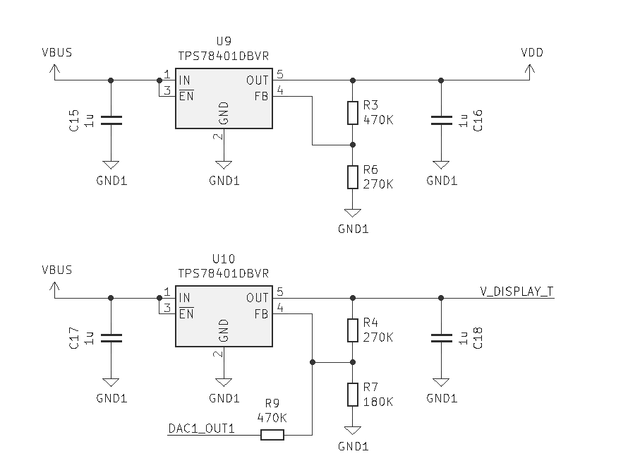
By my calculations, the fixed arrangement gives us 3.29V, and the variable ranges from 1.79V to 3.69V.
Confusingly, although not once you've thought about it a bit, the output voltage is highest when the DAC line goes lowest, and vice versa. This is inconsequential as we're applying a non-linear gain curve anyway.
One last point to consider is what the resting voltage will be. When the processor is in reset, the DAC is turned off and we revert to just the potential divider, which with 270K/180K will settle on 3.00V. That's fine, a medium brightness. In future, we could potentially add another resistor, a pull-up or pull-down on the DAC line, which is drowned out in normal use but holds our brightness to a known value when the DAC is turned off.
A note: this feedback-bending technique can equally be applied to switched-mode supplies. I'm not the first person to do this. Several times in the past, when I've wanted to add remote control to an off-the-shelf buck module, I've just added a resistor into the feedback network to gain voltage control over it. The reason I went with linear regulators here is that they're electrically quieter, and cheaper.
On the processor side, we set up a timer and double-buffered DMA transfers to the DAC. In addition to reading the ADC and non-linear mapping it, we apply a healthy amount of filtering, essentially a lowpass filter with a cutoff of about 2Hz, so it takes about half a second to react to light changes instead of bouncing around instantly when the sensor is covered.
Colon control
Since the Mark II, I've used the blinking colon separators to indicate the presence of a GPS fix. In fact, for the previous clock they also functioned debug data about the oscillator discipline. The new dynamic precision shows us if we've drifted more than a millisecond, but nothing beats the assurance of a signal to indicate PPS within the last second.
But not everyone likes the harshness of the blinking colons. It was certain that they should be configurable this time, but better than that, we want them to do a smooth animation, perhaps a fade in and out. They still need to dim with the overall brightness of the display.
I made the executive decision that stability at high frame rates is not critical for the colons, and that we can use PWM to dim them. Combining that with the voltage control of the main display, the PWM at max duty should be as bright as the other segments. This is surprisingly easy to achieve, now that everything's voltage controlled. I connect the anode of each colon LED to the variable voltage, and the cathodes, via limiting resistors, to GPIO of the microcontroller, with hardware timers configured for PWM output. Even though they're CMOS, at logic high level no current will flow (and at anything other than max brightness, the LEDs will be reverse biased).
As with, well, everything, we set up a DMA stream to clock data to the duty cycle. A two-second 100Hz buffer was used, meaning we can configure any arrangement of colon brightnesses we like for up to two seconds. That might be a simple on/off with each alternating second, or fading in and out, or what I ended up leaving as the default, a staggered fade in/out that suggests a heartbeat. More modes might be added later.
Since they're not matrixed and only low-side switching, the colon LEDs are not driven via the buffer chips. It's fine to drive a few LEDs from the GPIO, it's only an issue when the sum total current through the microchip approaches the limit, which it would if we drove everything from it. Similarly, on the date side, I didn't have enough pins on our three buffer chips to drive everything through them, as it's ten digits with decimal places. I chose to drive the decimal places directly from the microcontroller there. As usually only one decimal place is illuminated (if any, on the date side), there really won't be much current here.
Hinge development
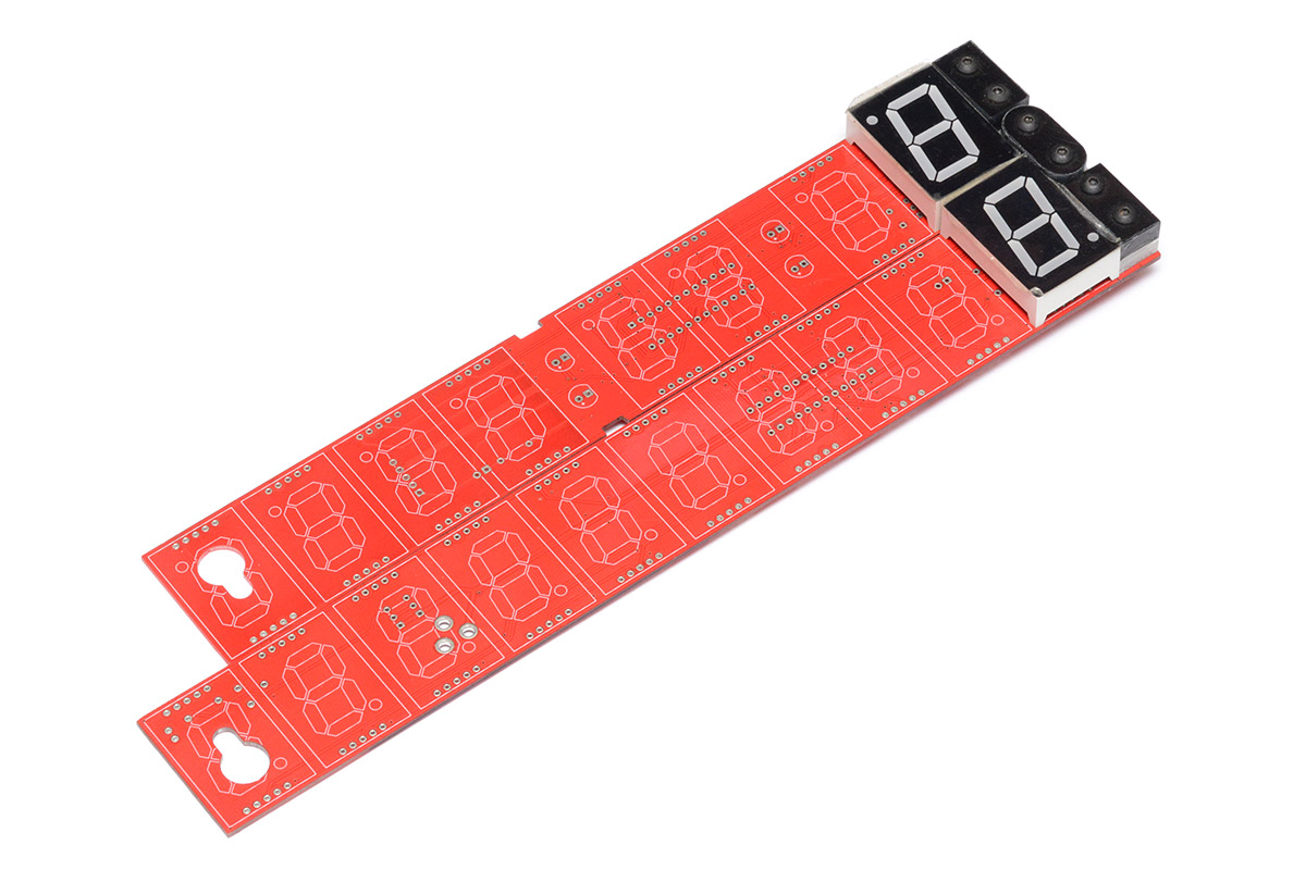
One of the most irritating things about the earlier clock designs was that the PCB was so long. If anyone wanted to buy a bare PCB, the cost of shipping just one was prohibitive. Some shipping rules jump from "small" to "medium" if any one dimension is longer than 50cm (which the clock was, just). It always amused me that I could potentially save on shipping by placing the PCB diagonally in a "small" box.
Splitting the circuit into two pieces was something I had in mind from the start, but the idea of an articulated joint, once it had occurred to me, did not go away. Realistically, nobody needs it to dynamically transform, but oh, what a swell feature to have. I think it was the request for a Precision Clock Clapperboard that made it stick. With the plan for automatic timezones, that middle portion of the clock is now dead weight anyway, and if we're millisecond precision, the widths will match perfectly too... it had to happen!
I took one of the old clock PCBs, sheared it in half with the tin snips, drilled some holes, filed the edges, and concocted this laser-cut prototype.
The vague idea was to paint a white line along the edge of the three sections. In the folded position, it would simply be a vertical line, but in the open configuration, it would spell out a capital T. I forgot about that when we switched to Delrin as a material, which is basically impossible to paint, but it has the benefit of being much stronger. Possibly excessively so. With the hinge made of Delrin, I'm pretty sure the PCB is going to snap well before the hinge gives way.
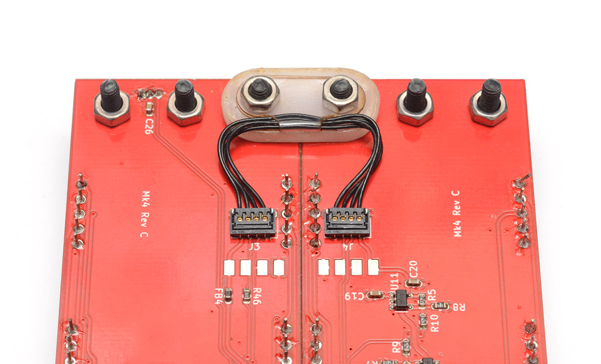
The electrical connection, of how many wires we can get across the hinge and what their impedance and current capability is, dictates quite a lot of the system architecture. There are a bunch of wire-to-board connectors available and I've had mixed results with several of them. I eventually settled on the Molex Pico-EZMate system. The hinge prototype was again used to try and find the best placement for it, with my initial plan something like this:
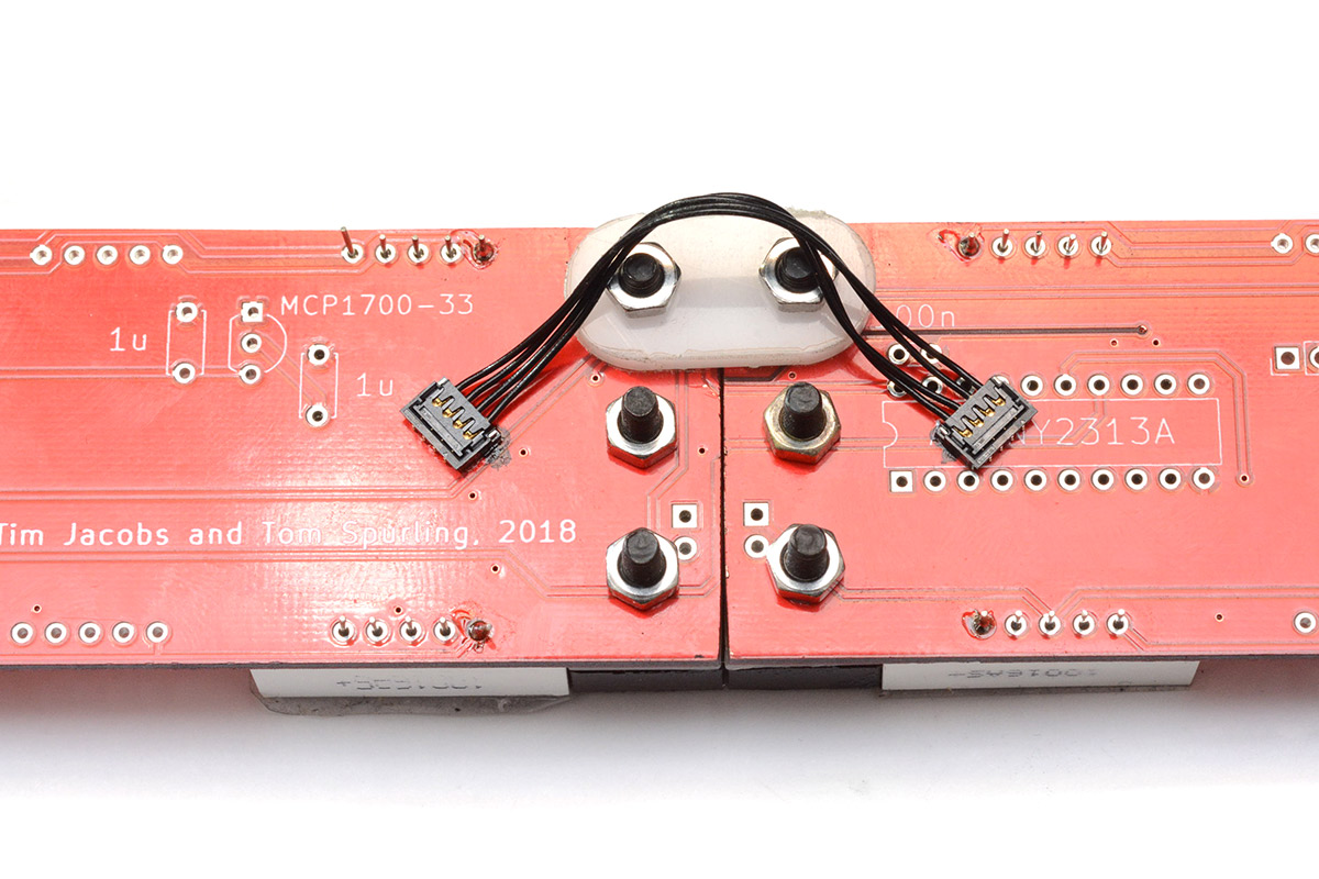
This worked but the cable was free to flop about, so the later design added the acetate cable support, and moved the connectors up appropriately.
This same concoction was used to prototype the placement of the hall sensor and magnet, to detect folded status, and then even, much later, to prototype the 3D printed colon holders with their plastic snap-tabs.
I've now confirmed the board-to-board cable to be quite reliable, but the paranoia at the time was that the hinge would fail in some way and make the clock unusable. I really dislike wire-to-board connectors that can't be hand soldered easily. The Pico-EZMate connectors are not too bad, but still tricky for a beginner, so for a foolproof method, I made sure to add big test pads behind each connector on the PCB, so in the worst scenario we can just solder wires across the hinge.
An unfortunate consequence of using the digits themselves as the end-stop of the hinge, that only became apparent much later, is that different suppliers of digits put the pins in slightly different places. My first prototype fit the digits I had to hand perfectly, since it was made to measure, but much later, as I built clocks with other digits, I had to bend the legs to get the plastic parts flush.
There is at least one producer of digits with a design that fits perfectly, but sellers make no distinction between these subtle varieties so it's very hard to get the right ones.
The Two Layer Challenge
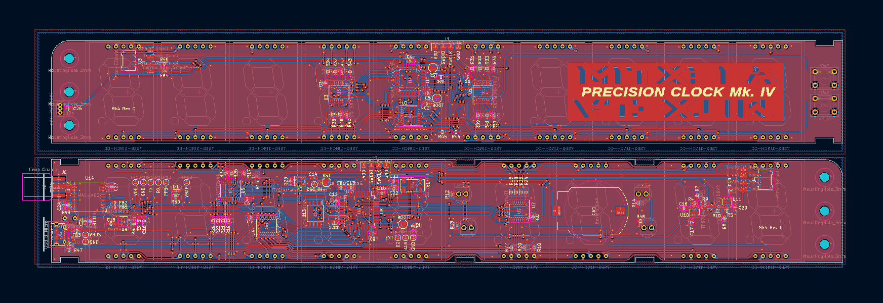
In the old days, having more than two layers on a PCB meant a substantial jump up in cost. Nowadays the difference, though still present, is not so significant and the idea of trying to be frugal with the number of layers might seem bizarre. Four layer boards have a multitude of benefits, even ignoring how much easier it becomes to route things. So I fully concede that my behaviour is irrational when I say that multilayer boards are a cop-out.
Artificially confining ourselves to two layers is exactly the kind of challenge I am wont to be engulfed by. The trick, if you want the board to work well, is to work on only one layer, and keep almost the entirety of the other layer as ground. It is almost always possible to do this, if you're willing to put in enough thought. I rather find that designing circuit boards is a lot like Tetris, and once I'm in the swing of it I can route things for hours on end. It can become a multi-day trance, with dreams of signal integrity and current loop area.
Not only did I want the circuit to fit within the physical bounds, I wanted the circuit to be beautiful. To this end I embarked on a multipart journey about melting KiCad. If you've perused mitxela.com at all in the last five years, you've probably been exposed to closeups and screenshots of the Mk IV clock PCB, which was the instigator of the whole thing.
The rounded tracks, the cubic bezier teardrops, melting the circuit as if it's dipped in honey – all of this was just for the aesthetics. The irony being that the tracks are too small to really be visible, but at least under a microscope, the layout is gorgeous.
The PCB was designed in KiCad 5, so all of the rounded tracks were done by subdivision, but here's a screenshot of the board loaded up in the more aesthetically pleasing default theme of newer KiCad versions:
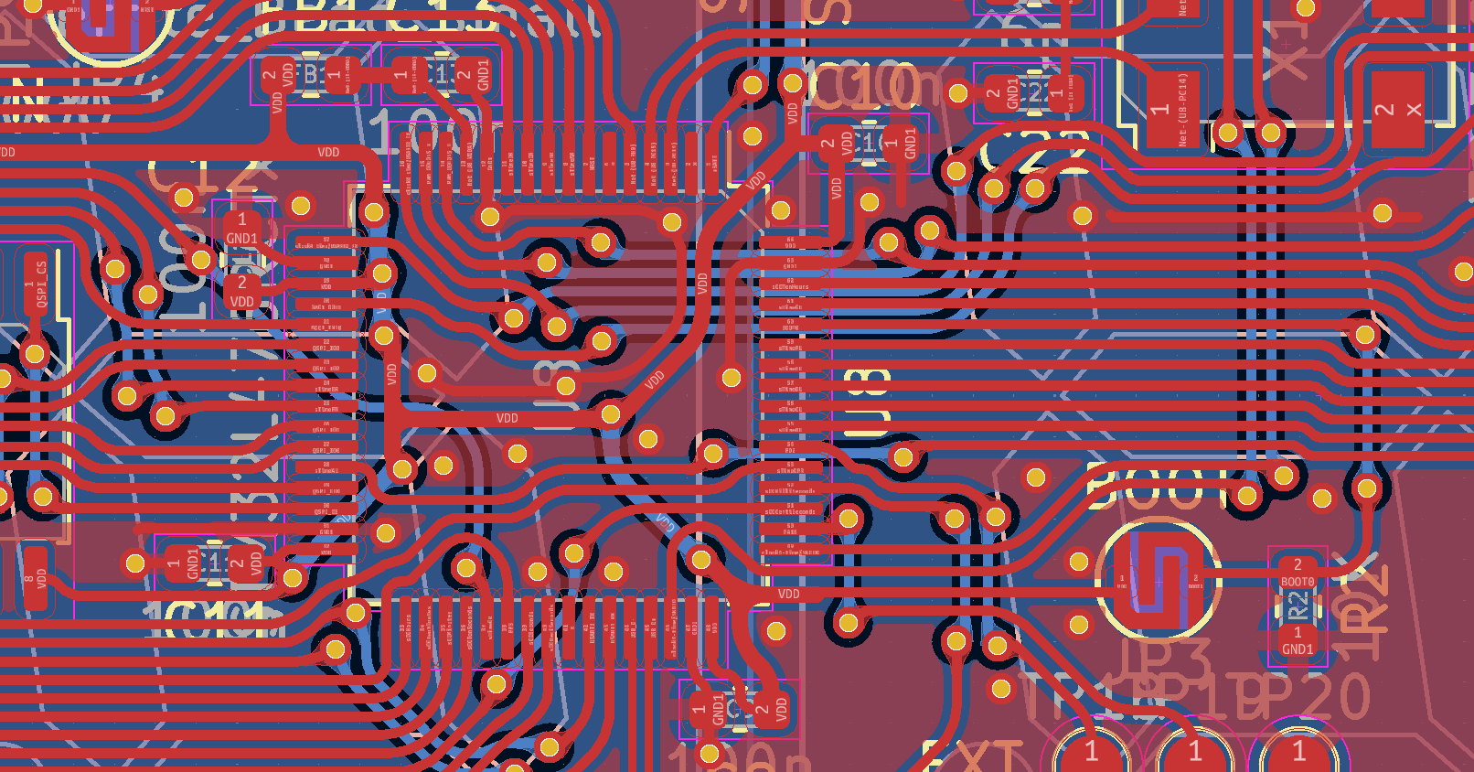
I mentioned the desire to route everything on one layer, which obviously isn't possible when it gets this dense, but a lot of thought was put into the ground plane continuity under and around the main processor. Ideally, the bottom layer would have been just tiny jumps amidst an otherwise unbroken ground plane. If signals really need to cross, they should do so at right angles, which I sadly wasn't able to pull off everywhere, but in these cases we at least think about what the signals are doing. The display signals are reasonably fast switching, the USB diff pair is fast but only used intermittently and reasonably robust anyway, the QSPI flash is fast but the traces are very short and direct.
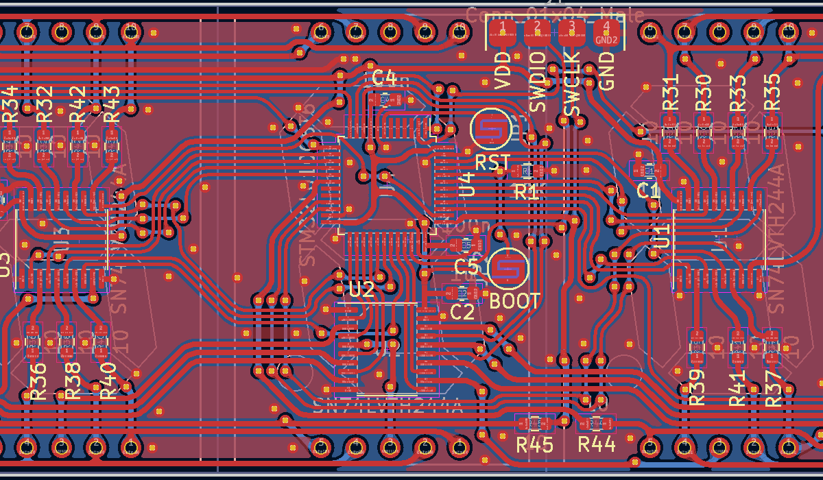
Some of the ground tracks within zones are to prevent me from accidentally moving other tracks and breaking the continuity there. Also visible in the screenshot above are the little pads I designed to act as switches for the reset and boot pins, which may need activating, but not often enough to justify fitting real switches. They can be shorted with a metal object if needed. It's very easy to make these too small without realising it: it looks big in the screenshot but the silkscreen around the pad has a diameter of just 3mm.
For a development board, it's possible to solder tiny tact switches onto these pads to make them easier to use. To trigger the system loader, you need to hold the boot pin while tapping reset, which can be fiddly, but it's not something that normal users of the clock should ever need to do.
I have a lot of self doubt when it comes to PCB nuances. A lot of people have very strong opinions about the "right" way to do a layout and I'm not really qualified to argue with them. The only thing we have to back ourselves up is the fact that the circuit boards work. But are they optimal? Do they benefit from the extra effort we're putting in? Would they, in fact, work, regardless?
Upon researching, I found some interesting opinions. One senior PCB designer challenged the common knowledge that differential pairs should be routed together. The total path length matters, but as for the individual lines, he claimed, it makes no difference. To demonstrate, he modified a board so that the USB diff pair split, with one line going up and around the top of the board, and the other going right around the bottom. The USB connection still worked. I'm not sure that's a completely fair test, but it at least proves that a lot of the worry is probably unwarranted. Another point made was about track thickness. It's conventional to make power supply tracks wider, for lower resistance and better current capacity. But unless you're pulling tens of amps, the heating effect of a thin PCB track is negligible. In contrast, said this one PCB designer, a thin track has a higher inductance, so if you make your power supply lines thin, you'll get a free bit of extra filtering.
I'm not sure what to make of it all.
Before finalising the interface, I was unsure how many buttons to add. I originally chucked three on there, but by carefully spacing the footprints, fewer switches would work too. Ultimately I went with the two buttons to cycle back and forth through modes, but even with two buttons, they're still spaced so that a single central button could be fitted instead.
If we wanted to do anything more than switching modes, such as capturing accurate timestamp signals, we'd want to patch that directly onto the time side PCB, so it doesn't have the latency of crossing the hinge. I put a couple of test pads near the main processor exposing the last of the GPIO pins.
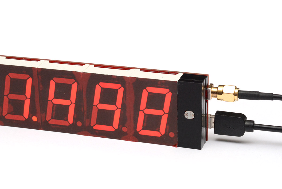
The first revision of the Mk IV PCB kept the simple header-pin mounting for the GPS module. This is pretty open-ended as there are a huge number of modules available with similar (but not exactly the same!) pinouts. The older clock kit was still shipping with the uBlox 6 modules, which are now quite old. At the time of development, the latest parts were the 8th generation uBlox modules, that have better performance, but the breakout boards for these had TX and RX swapped compared to the earlier pinout. This breakout board uncertainty, coupled with the fact that I wanted easy antenna changes, led me to solder the castellated module directly to the board with an SMA connector next to it.
The problem we then encounter is that the track between the SMA connector and the castellated module needs a controlled impedance. There are calculations for track width based on substrate thickness to get a given impedance, but if you run the numbers on a 2 layer 1.6mm board you'll find the track needs to be some crazy width, maybe a few millimetres. In addition, because no one attempts this usually, the dielectric constant of the FR4 is not well controlled for 2 layer boards.
Having said that, the breakout boards for GPS modules are usually 2-layer with little to no consideration given to track impedance. Often the antenna turns a few corners on the PCB with no apparent loss in performance. The fact is, at 1.5GHz, so long as the trace is fairly short it's not going to be a problem. Still, to be on the safe side, I made the track as short as physically possible, by mounting the GPS module in almost direct contact with the SMA footprint, as we can see on the prototype revision B:
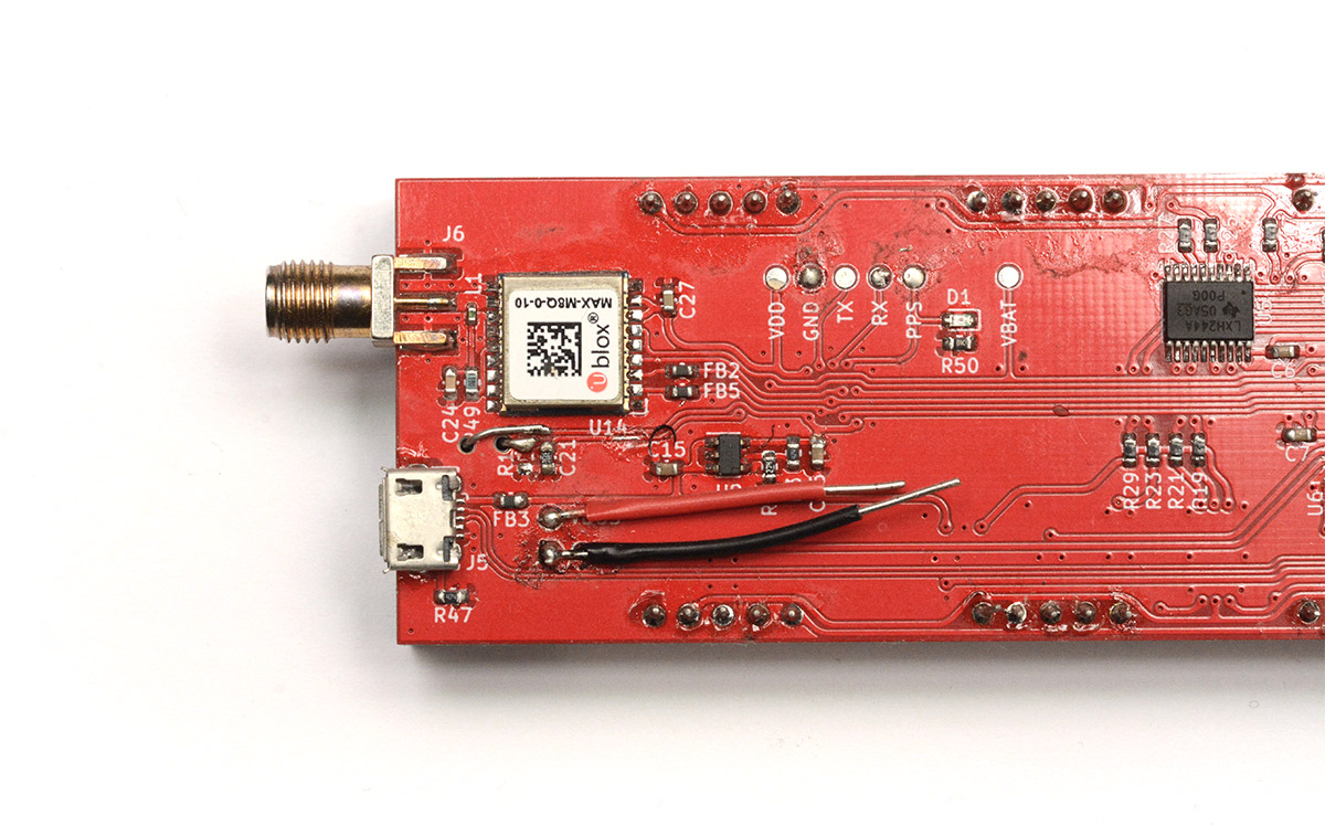
The tiny 0402 component is an inductor, that forms part of the RLC filter providing the bias voltage to the antenna.
Also visible in the picture above are two holes drilled to make a footprint for the LDR. I spent a long time worrying about the light sensor, even after we'd decided on how the digits were driven. The first revision of the PCB relied on an op-amp circuit. After dismissing that method, I mounted an SMD ambient light sensor (SFH5711-2/3-Z) but mechanically, topographically, this posed a problem. The light sensor obviously needs to point forwards, but part of my specification was that surface-mount parts are only on the back, and through-mount parts only on the front. Ideally, we could come up with some reverse-mount photodiode and a light pipe arrangement, but after fiddling around with this for ages I just reverted to using an LDR.
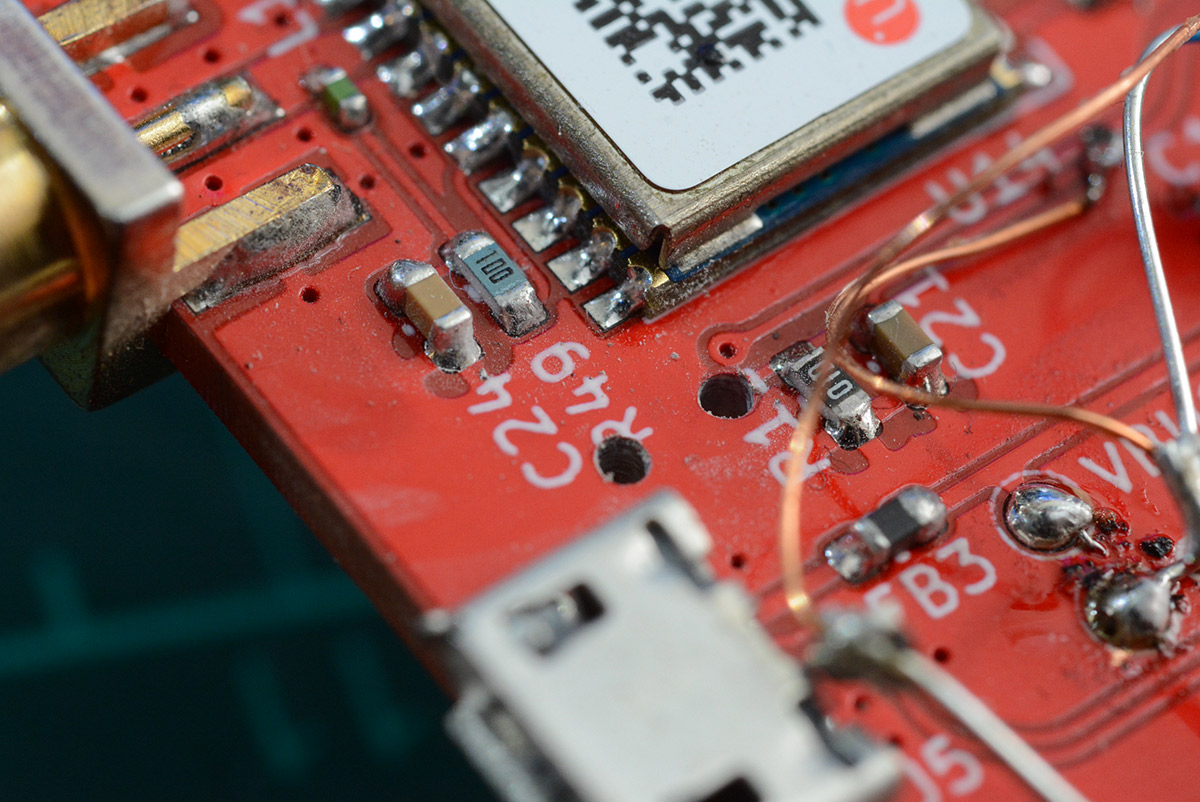
The one downside to this is that technically, CdS LDRs are not RoHS compliant as they contain cadmium. I kept the ambient light sensor footprint on the board as DNP in case anyone would prefer to fit that, but I think the long term solution would be to find a through-mount, photodiode-style ambient light sensor. This may happen on a later revision of the PCB.
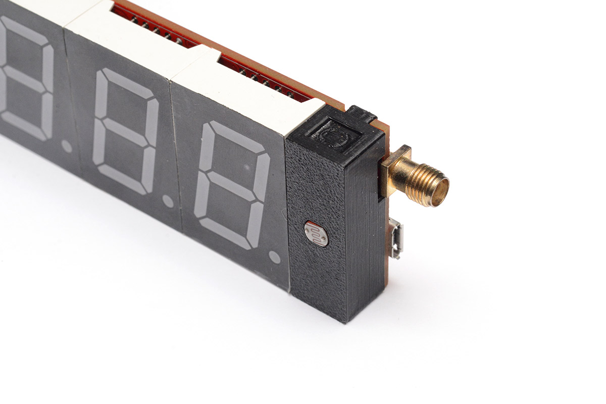
Plastic Parts
I am a huge fan of laser-cutting, and when it came to finalising the clock instinctively I turned to laser-cut parts. Instead of plywood that needs painting, or expensive delrin, for the non-structural parts of the clock I tried out matt black acrylic.
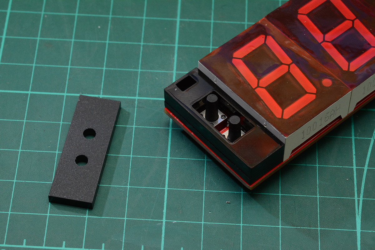
The hole at the top is for the magnet. Also apparent, on this prototype clock I applied red window tint film over the digits, to see if it was worth it (I decided it wasn't).
The matt acrylic looks great, but has the same problem as the parts in the old kit. To build up the shape, the layers need to be glued together, which I know from the previous kit is enough of a hassle that many people don't bother. Reluctantly I turned to 3D printing.
The 3D printed designs, with the addition of snap-tabs, mean we can avoid glue entirely. My only complaint is that printing them is very slow. On the other hand, unlike the laser, it can be set printing and left unattended, so in reality it's not so bad.
It took a few iterations before I was content. The magnets alone do an OK job of holding the clock together when it's folded, but they don't prevent the PCBs from flexing slightly, meaning the digits farthest from the hinge could slide forwards and backwards a few millimetres. To ensure they snap together and don't slide about, the joint was augmented with a recess, and a corresponding protrusion on the other end, so when the magnets snap together it grips tightly.
The texture on the face is from the printer bed, which I think is a nicer effect than without it. Unfortunately that means we need to print in the plane that gives us the weakest possible snap-tabs. That shouldn't be an issue, as they're not going to be subjected to much in the way of forces normally, and printing in PETG gives us a bit of extra strength anyway. We can potentially alter the design later if it turns out to be a problem.
Logo
Design optimisations mean that a fair amount of the date side PCB is empty, and represents prime real estate for a logo. But the date side is inverted when the clock folds in half, so our logo needs to look good in both orientations.
This predates the full-colour PCB printing options that some board houses now offer, and I wouldn't have gone for that anyway given the variety of visual interest we can create from the layers we already have. The silkscreen is white, the soldermask is red, we also have a darker red if we remove the copper from behind the soldermask. Exposed copper will end up either gold, or silver if we go for HASL finish. Finally there's the option of bare substrate material if we need it.
The idea of a "mitxela" ambigram didn't really appeal, I've always felt they're something of a gimmick. Instead, as you may have already noticed from the images above, I laid out the name twice with "Precision Clock Mk. IV" in silkscreen through the middle.
![]()
White is silkscreen, yellow is exposed copper. The shadows (which are intentionally not symmetric, as merely flipping it would look weird) are soldermask over bare substrate, i.e. keepout regions for the copper pour. I did the logo layout in inkscape, exported it as SVG and then attempted to import into KiCad using a tool called svg2mod. That tool has been rewritten substantially since I did this logo, but at the time it struggled to process it and I had to alter the plugin code slightly.
The task is to convert the arbitrary shapes of an SVG into distinct, closed polygons for KiCad. The main copper layer is essentially a rectangle with holes in it. Initially I tried exporting directly as keepout polygons, but this gave a subpar result and besides, having a rectangular border was desireable. But exporting to the copper layer directly means breaking up the holes in the shape into a single contour. Svg2mod attempts to do this by finding the nearest point, and slicing an invisible line, so that, say, a donut becomes a closed C shape. Lots of holes and only four corners to branch from led to some errors. I eventually submitted a pull request with my modifications for a recursive approach, but it turned out they were partway through rewriting the algorithm anyway.
![]()
A more pragmatic solution turned out to be quite easy, we just overlap the shape with a rectangle in inkscape and do a boolean modifier. That lets us manually split complex shapes into smaller, closed pieces and the conversion process doesn't need to worry.
The stylised logo is in a font called Cyberdyne, by Dan Zadorozny. We do enjoy their 2007 webpage layout.
The logo was something of an uncertainty until the first PCBs arrived. I was reasonably pleased with the result. The HASL finish has a mirror-like quality, which I expected to dull quickly but these boards seem to have held up pretty well.
![]()
Countdown mode
With the ease of firmware updates, we could have delayed most of the software development until later, especially for secondary features like Countdown Mode. The logical thing to do would be to release the clock as soon as possible, and add these bonus features later. It's apparent that I'm not really a logical person though.
Countdown mode is something of a mind-bender, as simple as it may seem. Just display the number of days, hours, minutes, seconds until an epoch. But the precision, and the dynamic precision, make this a far more subtle problem.
To be clear, a normal wall clock does not "round" the time display, it "floors" it (round-down). The last digits of precision are truncated. This has to be true: if the time is 3:59, we might colloquially say it's 4 o'clock, but a digital clock would not display the number four until the exact moment of 4 o'clock is in the past. Further precision, of seconds and subseconds, doesn't have any bearing on when the hours digit ticks over.
Think about New Year's Eve where people count down to midnight. They might say "3... 2... 1... Happy new year!" In other words, the event happens when the seconds remaining reaches zero. But consider a countdown with fractional seconds. At 3.x seconds remaining, we'd say 3. But when the whole seconds reaches zero, we still have a 0.9... fraction remaining. The exact moment that the whole seconds ticks down to zero, there is one second left until the event.
I don't think we'll be able to convince people to do their New Year's countdown as "3... 2... 1... 0... Happy new year!" but that would make an awful lot more sense. By truncating digits off a count-down, we are "ceiling" it (round-up), and it can never precisely display the moment of the epoch. Our precision clock displays to the millisecond, so you would think the event happens when it ticks to 0.000, but in reality, it should be one millisecond after that.
This was essential to get right, as the dynamic precision of the clock otherwise wrecks havoc on when the moment is signified. If we've lost GPS fix, or maybe the clock's been powered off for a while and only showing to whole seconds, should it display the whole number of seconds rounded down? That'd satisfy our New Year crowd but not the scientists in the audience. And what if it then gets its GPS fix and can display to the millisecond, do we then alter that number of whole seconds remaining? I think not. The only thing that makes sense is to truncate, rounded up, and spread the word that everyone's doing their countdowns wrong.
Leap seconds
Officially a digital clock should display the number 60 during a leap second.
After a bit of research, it seems that GPS modules are wildly inconsistent in their behaviour during a leap second. I eventually concluded that the safest thing to do is to prepare, in advance, a list of upcoming leap seconds and during that second, ignore the GPS module.
The list of upcoming leap seconds is available as part of the timezone database, and since we already need to keep that up to date, there's not too much overhead in doing it this way. The only thing is that some people may not ever update the database, especially if they live in a country that never changes its timezone rules.
When I started writing the firmware, this was my plan. But the drift between UTC and UT1 suggested there wouldn't be a leap second for a long time, so I put this at a lower priority. Eventually, in the last few years, the difference became such that it was suggested to have a negative leap second, which has always been possible but has never happened before.
If you'd asked me, we should have redefined the second orginally so that all leap seconds were negative. Skipping 59 is so much easier than adding a 60. And the Unix timestamp would skip a value, instead of repeating a value and being ambiguous. I think everyone knows what adding a negative leap second would do to the world though, and an announcement was made recently that leap seconds have been semi-retired. Instead, we'll have a leap minute when that becomes necessary. Thus, the problem has been thrust upon our great grandchildren, and thankfully when that happens we'll all be dead.
I could say a lot more, but with regard to the clock, if another leap second is ever announced I will implement the feature and release a firmware update for it.
High speed testing
While developing the previous clock, I invested in a consumer camera that could shoot at 1000FPS. It was exactly what I needed to debug and confirm the operation of the seconds interpolation.
I got the Mk IV display working without much issue, but 1000FPS is not actually sufficient to confirm its operation. I felt confident, partly because of the interference effects I was getting through the viewfinder of the camera. The preview decimates the framerate, but apparently it's exact, showing only every tenth frame. As such, the milliseconds digit of the clock appeared to be completely solid, unchanging.
The really cool thing about this is that there's still a rolling shutter effect, so as you tilt the camera up and down, with the clock being in different parts of the frame, the number shown on that static last digit changes.
But I wanted to be sure, and started asking around. It turns out that companies that own high speed cameras are surprisingly amenable and enthusiastic when people turn up and say they have something cool to film at high speed. Huge thanks to Pirate for giving me some time on a Phantom Flex 4K.
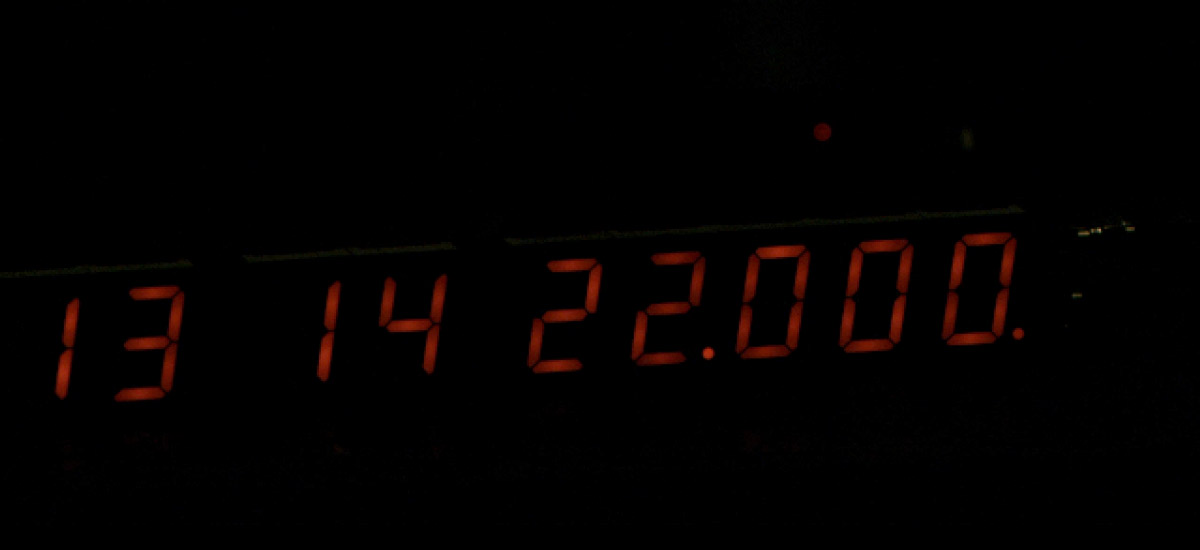
Even the memory cards for this camera cost as much as a house. In the freeze frame above, the real frame rate was 2932FPS at 1080p. The last decimal point was being used the debug the interrupt timing. The red dot above the clock face is the PPS LED. To as good as I could tell, the clock was ticking perfectly.
I later found out how to activate the higher framerates of the camera, so in a later session, we filmed the clock first at 14,000FPS:

and finally at 25,000FPS, the highest it will go. At that speed the frame is just 16 pixels high, which was enough to see that the time was displayed perfectly. Note that the camera used a shutter angle of 180°, so the effective shutter speed was 1/50,000th.
We'd already confirmed the accuracy of the PPS LED with respect to the UTC second, and now the display was confirmed to be aligned to the PPS LED. Proper job.
I also, for fun, turned down the matrix update speed. We were able to slow it right down, and film the matrix progressing, and also set the matrix speed to match the camera framerate, which leads to a beat frequency as their relative oscillators slowly drift apart. In that situation, the beat frequency of the time and date sides differ, as the date matrix frequency is derived from the internal oscillator of the date side chip, while the time matrix frequency is based on its highly accurate TCXO. I briefly looked into disciplining the date side's oscillator to the highly accurate latch signals being sent across the hinge, but the internal oscillator calibration is quite low resolution so it's probably not worth it.
Travel testing
For the entire development period, the clock existed only on my desk. The automatic timezone detection worked in theory, and it's possible to feed it fake GPS coordinates, but that's not exactly the same as proving it works. When the opportunity arose to take the clock abroad, I had to take it.
I first took it to the Dutch hacker camp, MCH2022. I had very much hoped to be able to watch the timezone update while riding the Eurostar. Unfortunately, the metal structure of the train completely blocked the GPS signal, and it wasn't able to get a fix until we departed. Aside from that, it all appeared to work.
Later I was given the chance to take the clock to Greece. The idea of taking the clock on a plane, and watching it update as we flew across the timezones, was particularly appealing, but ultimately I decided to keep it in my luggage, as the large red ticking digits do have a resemblance to a cartoon bomb.
One morning, in the natural harbour of a Greek island, I unfolded the clock and powered it up.
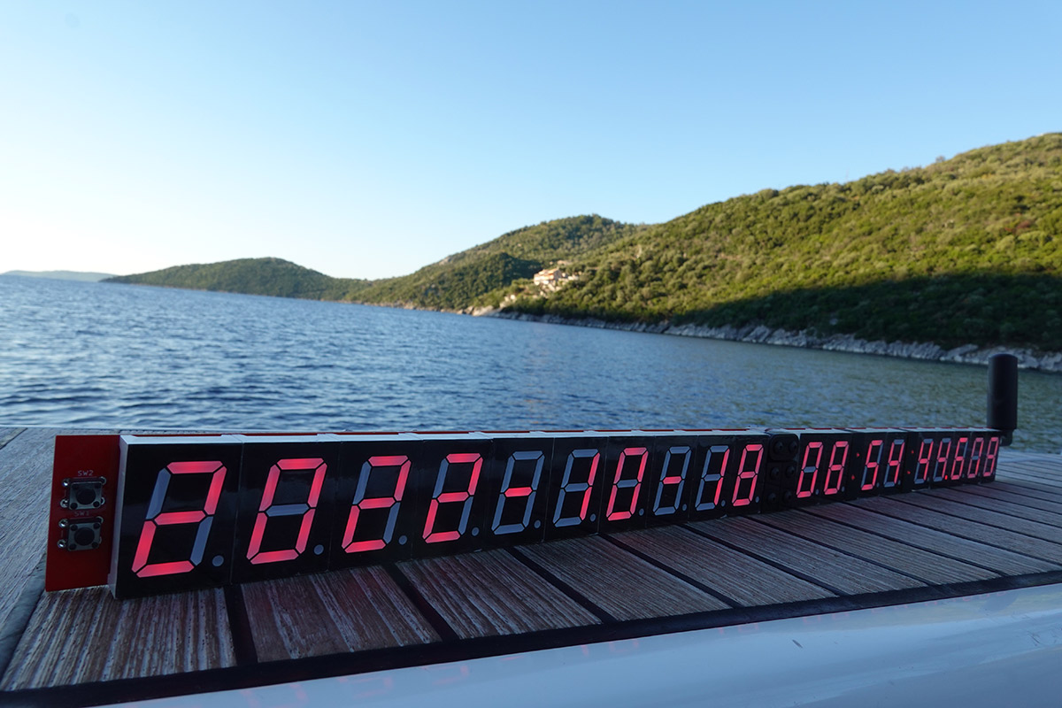
This was the Rev B PCB, with the "stubby" antenna. Clear skies, so it updated to the correct UTC offset of +03:00 almost immediately.
My ambition was to sail out to sea, and find somewhere with no cellular phone reception – somewhere that only our GPS Precision Clock could serve the time reliably. Unfortunately, there's fantastic phone signal between all the islands so we couldn't actually find anywhere that it mattered.
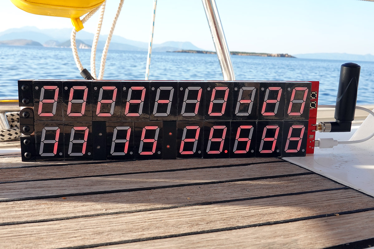
Still, we proved the clock worked at sea!
The digits were a little difficult to make out in the Mediterranean sun. For Rev C, I slightly boosted the max brightness, although direct sunlight is always hard to compete with.
The production batch
As I geared up to sell the new clock, a global chip shortage happened which meant producing it was, for the moment, impossible. There are horror stories about multi-year lead times, paying ten times the normal price, and still not getting the delivery because someone else outbid at the last minute. Everyone sensible redesigned their circuits to make use of parts that could actually be bought. I didn't have the heart.
When the STM32 chips finally came into stock, at a significantly inflated price, I tentatively ordered 100 of them. I wasn't really thinking about how this would work. For a kit, it wouldn't really be fair or practical to send out unpopulated circuit boards with dozens of fine pitch surface mount components to fit. The only viable clock kit would be if the SMD parts were fitted, and just the through mount and mechanical parts need assembly. I had originally planned to order the populated PCBs from China, but sending my own parts out there is completely impractical. Aside from anything else, I'd end up paying import/export duty on everything repeatedly.
When a pick and place machine was donated to the hackspace, however, an idea occurred. Possibly the only benefit of the hackspace being evicted from their building is that everything had to go into storage for a few years. I helpfully offered to "store" the pick and place machine at my house.
The machine is a Charmhigh CHM-T36VA.
I've since featured this machine in a few projects. It directly led to the volumetric display and the badge, and I pushed the limits of it with the matrix earrings. Anything with a large number of similar components is very easy to set up and produce. But if you have the patience to load all of the reels, the machine can be used to produce complex circuit boards too.
There are 26 unique surface-mount components on the clock, which means 26 reels. The machine has a number of fixed-width feeders: the first twenty-two are 8mm, then four at 12mm, two at 16mm and one 24mm. That's enough to hold almost (but not quite) all of our parts.
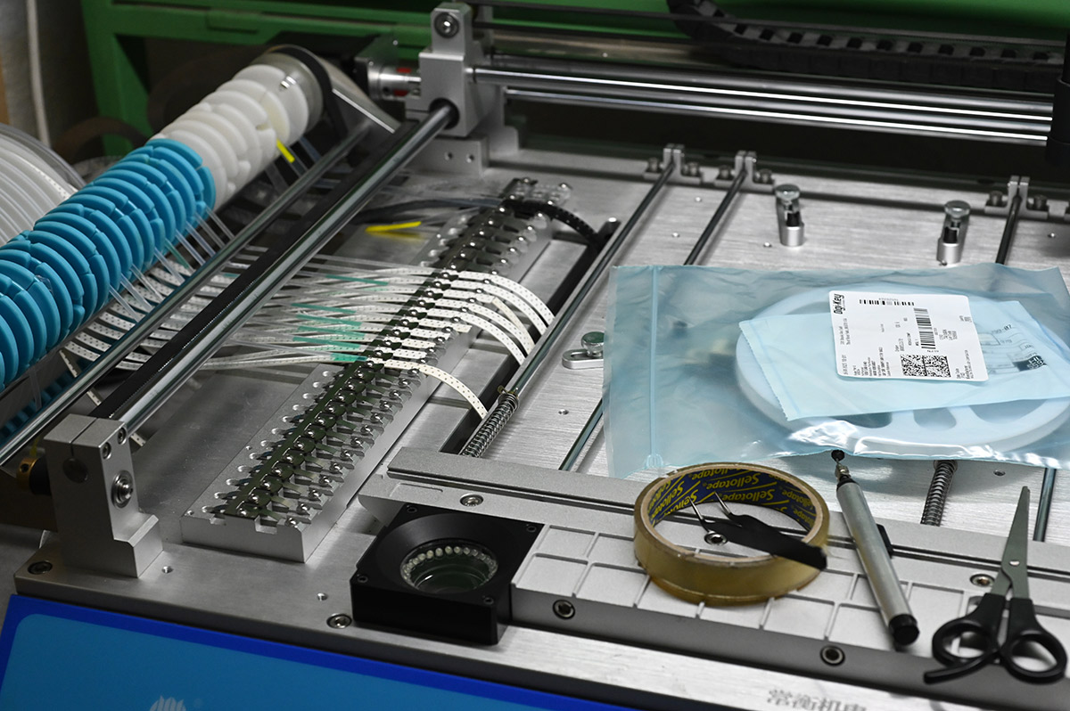
Loading a reel is a tedious affair. The film needs to be peeled back enough to reach the take-up spool, which usually means joining onto the previous piece of film. There are tiny stickers available that can be used for this purpose. The sprocket holes need to align to where the machine expects them, and the waste tape needs to be guided down into the slot, when enough of it has been exposed.
I ordered most of the parts from digikey. Like several other distributors, they offer a re-reeling service, so if you buy less than a full reel, and are willing to pay a $5 surcharge, they'll attach a leader to it and put it on a reel. I went with this as I thought it would save time. It turned out to be completely and inexplicably useless.
They obviously have the technology to join two pieces of cut tape together. That is how the leaders and trailers are attached. And yet, what they sent me was a total mishmash of reels with random amounts on them. For one part number, they sent three separate reels, one of which had only four components on it! Given what a palaver it is to load a reel, this is actively unhelpful.
Additionally, the brass shimstock they used to join the leaders was pretty poor. It was both weak enough to easily break, but thick enough that it tended to jam in the feeder. It's perfectly possible to load cut tape into a feeder, you just need to advance it enough to be able to attach the film to the take-up reel.
Another pain in loading the reels for the first time is that you need to carefully note down in a spreadsheet what's been loaded, the part orientations, the feed spacing and so on. The machine will accept quite a few parameters for each feeder, such as which head to use, whether to use the vision system, whether to check the vacuum pressure, centroid position correction and so on.
The big ICs were shipped in a tray. There's provisions to clamp a tray into place and instruct the machine on the array of parts. I was reasonably impressed with the ease of setting this up.
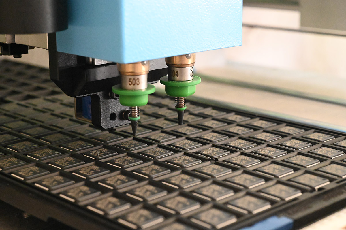
The machine software is intended to run on a dedicated tablet, and has a pseudo-touchscreen interface. Some idiosyncrasies arise from this, such as the software being unable to talk to anything except "COM1" on the windows machine. I had to tediously redefine the COM number of the serial port in Device Manager. Another, somewhat comical effect is that it assumes the first two video devices are the vision system. The laptop's built-in camera had to be completely disabled to avoid this. Powerup is also sensitive to the order in which the USB cables are plugged in, get it wrong and the cameras don't work.
It's a bit clunky but defining an IC tray amounts to x,y coordinates of the first and last component, and how many there are. The vision system lets you line up the parts through the GUI. The software keeps track of which parts have been picked during use and is surprisingly robust. For the parts I couldn't fit into feeders, I laser-cut some holders for them out of plywood, effective turning cut tape into single-row IC trays.
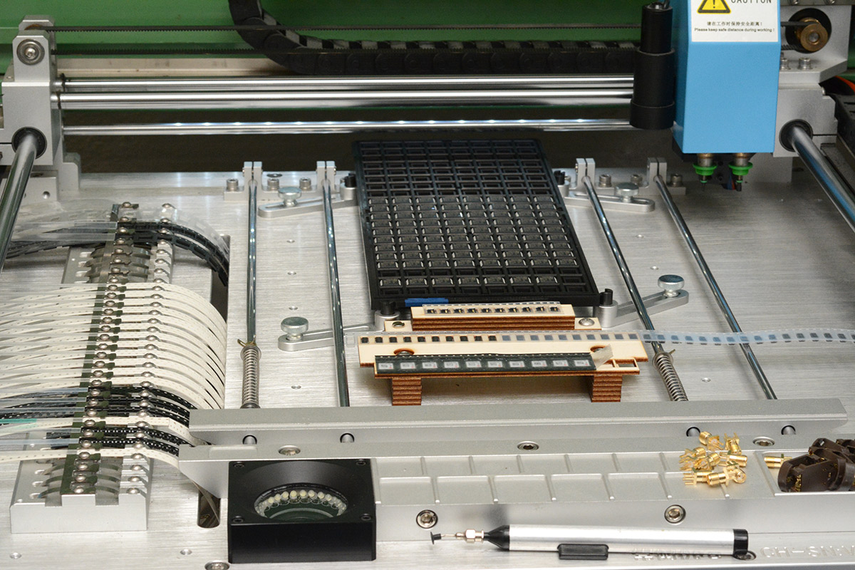
For the two most awkward parts, the coin cell holder and the SMA connector, I just placed these by hand at the end.
A nice feature is that you can step through a job one motion at a time, and check everything's working.
When we're ready to go, it's time to stencil some solder-paste onto a board, and start placing parts.
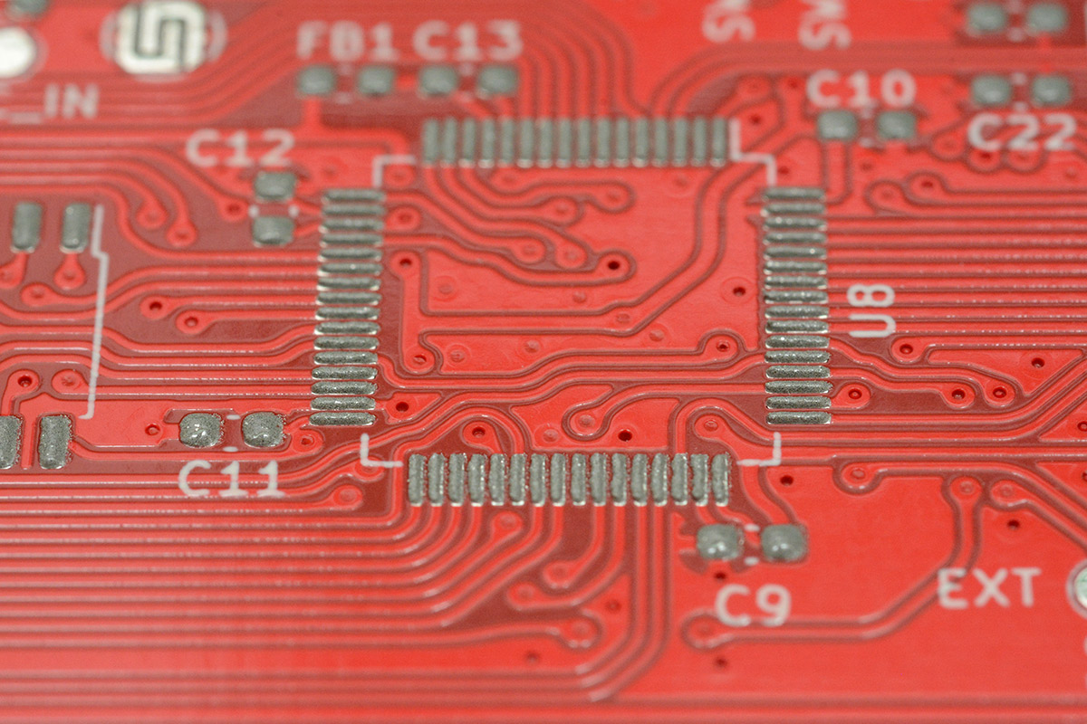
There's a knack to stencilling paste well. Something I quickly figured out, when it came to making the batch, is to frequently wipe the underneath of the stencil. If the tiniest bit of paste pulls astray as you lift the stencil, it will get jammed on the next iteration and stop the stencil from sitting perfectly flat. This leads to more stray paste under the stencil, and it quickly spreads to being a total mess. A simple wipe with a paper towel on the underside keeps this from happening.
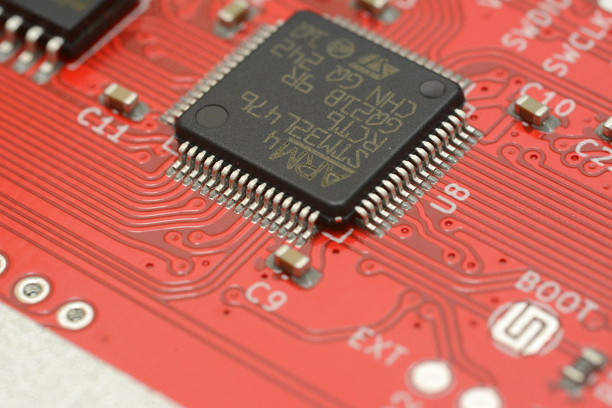
The smallest part is our 0402 inductor, and the largest part is one of these integrated circuits. There's no automatic toolchanger on the machine, but the two heads are just about enough to cover everything. I pretty much grouped it into two categories, small things and big things. Using too-small a vacuum nozzle means parts are likely to twist as they get grabbed. After picking up a part, the machine holds it over the up-facing camera and determines the outline.
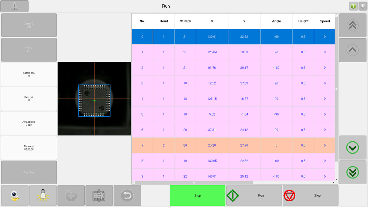
There's no information in the feeders list about part sizes. It has no idea if what it's holding is a tiny resistor or a big IC. It just draws a box around what it thinks are the pins, finds the centre and angle, and corrects for it as it places the part.
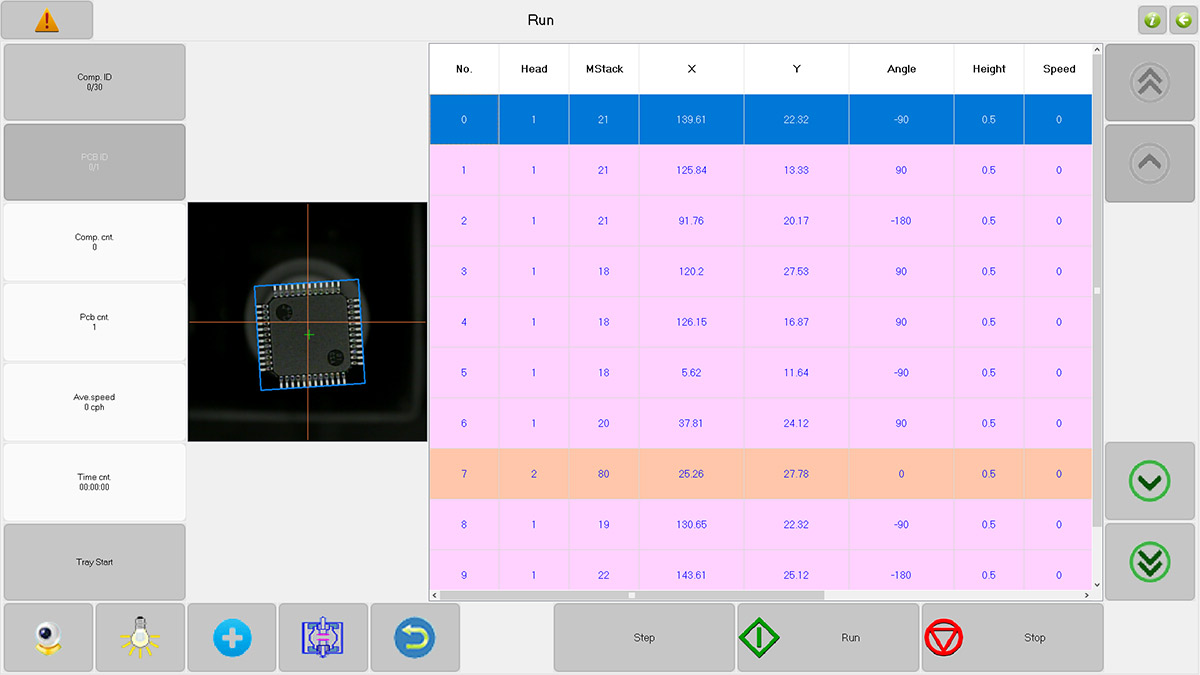
A problem I had early on is that stray light interfered with this, sunlight from the window and the big fluorescent light of the desk caused reflections. Sometimes it would think a small resistor was a big chip with a pin over in the corner. The addition of some black tape on the carriage solved this entirely, so that seems like a design flaw.
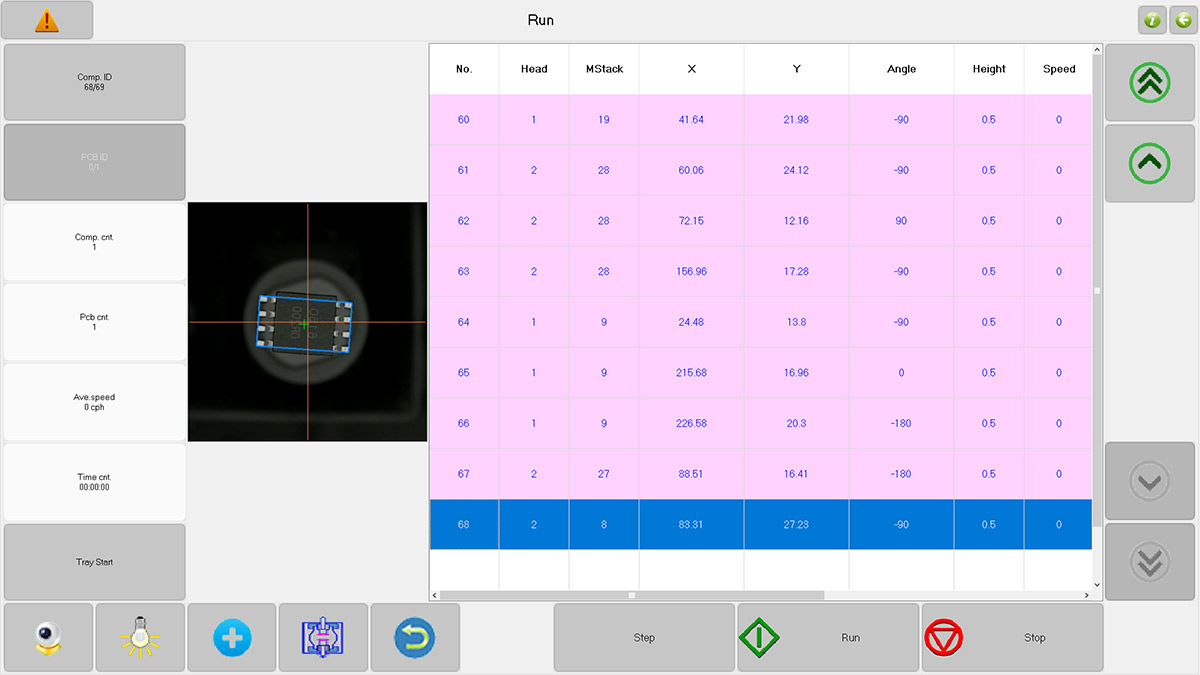
For the most part, once I got this working, it worked great.
After placement, the boards need to be reflowed (cooked). The pick and place machine, both its donation to the hackspace and my temporary procurement of it, came with a reflow oven. This oven is a monster. It weighs a ton, draws 3.5kW, has a conveyor belt and six PID-controlled temperature stages (three top, three bottom). If anything, I think I would have preferred something smaller and better matched to the speed at which I could stencil boards and place the parts.
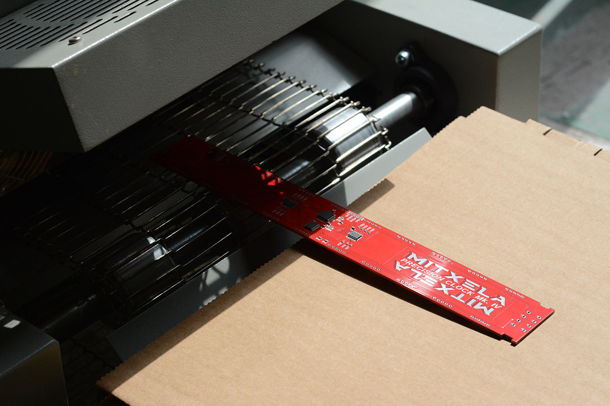
One tiny disadvantage of reflowing is that the HASL finish of the beautiful logo gets a little tarnished by the process.
I didn't experiment too much with the settings for the oven. I realised midway through that one of the fans was stuck, and after dismantling the machine I was able to repair it. I think this was the reason that the previous user had set the temperature a lot higher than it needed to be. Speed of the conveyor is quite important. The hardest part to get to reflow was the GPS module, with its shielding can.
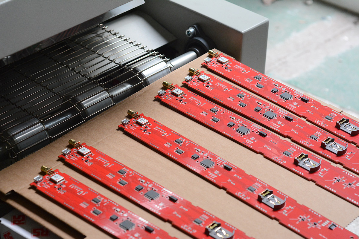
The cardboard is my cooling surface. The conveyor by default just dumps the boards on the floor. At least twice, I wasn't watching the output and a board got caught in the conveyor and pulled into the machine, in one case breaking the SMA connector. The need to supervise it is a huge detriment to the throughput. What I ended up doing, once I'd got the speed right, is setting a timer every time I put a board in, which would go off a few seconds before it came out the other end.
Honestly, for these 100 sets of clock PCBs, I think doing them in batches of 10 or 20 in a normal oven would have been much more sensible.
The thing I regret most about this batch is that I used up the last of a pot of solder paste I already had. I only planned to do a test run with it but since it worked fine, I continued through the whole batch. Towards the end, the paste had definitely expired. For the most part this doesn't matter, it just means the joints are not as beautiful as they could be. It was lead-free solder, as I was trying to be RoHS compliant, so they would never be that pretty, but since the clock PCB sort-of puts the parts on display I would have preferred them to be as nice as possible. Given how much I invested into this, it's silly that I didn't buy a fresh pot of solder paste for the batch.
Moreso, I learned that the fumes from lead-free solder are horrible thanks to the much more aggressive flux it requires. The oven has provision for proper extraction, but on the first day I didn't pay much attention to this and ended up with a splitting headache which knocked me out for most of the next day. I probably hypersensitised myself to it, as even after installing the proper ducting, getting a whiff of the flux fumes would cause my brain to swell.
There's a lot I've skipped over here. For instance sourcing the GPS module was a nightmare. It was out of stock everywhere, but a seller on aliexpress listed them. I bought two initially to check they were OK. The two parts sent to me appeared to be genuine and worked perfectly. I then ordered a hundred, and what arrived were one hundred fake GPS modules that didn't work. They had the same sticker on top but the PCB design was subtly different, and, well, they just couldn't get a GPS fix. It was a colossal waste of time and money (which I never managed to claw back from aliexpress – they wanted video proof of all of them not working simultaneously).
I eventually found someone in the UK with an unopened reel of genuine parts, which they were willing to sell to me. What's the lesson in all this? I don't think there is one, sourcing parts is a nightmare at the best of times and sourcing them during a global pandemic was excruciating. As a final slap in the face, after fighting through all this I then lost momentum and waited long enough before releasing the clock that the supply chain problems were resolved, and these parts are now available for a lot less than what I paid for them.
Conclusion
Congratulations if you've read all of this, it must be one of the longest project pages on the site. Writing it up took only a few days. Developing the clock took years!
I've had a Mk IV clock in every room of my house for the last few years, and one thing that has really grown on me is the dynamic precision. Being able to immediately see the tolerance is invaluable.
There's an old adage that a man with one clock knows the time, but a man with two clocks is never sure. Unless, of course, those clocks display a tolerance.
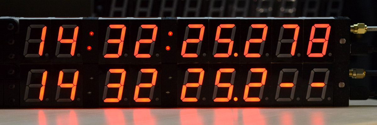
I showed off the clock at EMF 2022, and then, two years later at EMF 2024, I did a talk on it and the development that went into it. That talk is available on media.ccc.de and youtube.
It is weird to think that there are almost a thousand Mk III precision clocks out there. Throughout the development of the Mk IV, I tried to incorporated every feature request I'd ever had, and there are only three things that I couldn't squeeze into the Mk IV.
- One was to make the clock waterproof. Both for outdoor usage, and in one request, to be fully submerged. The hinge design complicates this greatly, and I decided the best option for waterproofing is to put the whole clock inside a sealed clear box.
- Two was to give it a lithium-ion battery. I did consider adding a charge controller and the footprint for an 18650 holder, which would have turned the clock into a self-contained thing with no cables, but for the vast majority of use cases it's totally fine to connect up a USB battery bank.
- Three was to give the clock even more precision. There aren't many people that have access to cameras that can go above 100,000FPS, but one rather prominent person asked me to build a clock that would read out to the microsecond. We did some tests, and it's absolutely doable, but I promised I would release the millisecond clock first.
For the Mk V, or whatever I call the microsecond version, it'll not only need direct drive of all the digits but the ability to go a lot brighter. At those frame rates we need a lot of light, so we might need a boost button to temporarily up the current. I may as well share some screenshots of the single-digit prototype I built, first ticking glacially slowly at 100000FPS:
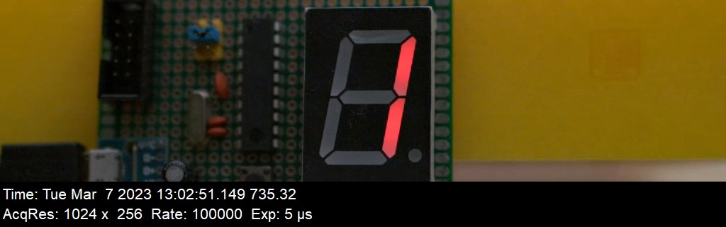
and finally ticking at one microsecond, filmed at an incredible 1.75 million FPS:

Naturally if we did build this full clock, we'd need to put a bit more thought into the time source, as the basic GPS modules have a sawtooth error on the PPS that would start to become significant. There are timing-specific modules with more stable outputs, or we could go back to disciplining a local oscillator. It's important that the microsecond digit has a jitter of much less than one microsecond.
Anyway, that's in the future. To conclude this conclusion, I'll just say what a relief it is to finally publish this. The source code to the clock is in the github repo where many of the commit messages contain even deeper technical info. The PCB files will also be published soon.