.png)

Introduction
Optically addressable solid-state spin defects are versatile tools for quantum-enhanced technologies1,2. The photonic degree of freedom enables single-spin readout3 and control4,5 and entanglement generation6,7. Moreover, engineered nanophotonic structures can greatly enhance spin-photon interfaces, where customized structures such as cavities8,9,10,11,12,13, solid immersion lenses14, metalenses15, nanobeams10,16 or nanowires17,18 can be fabricated in the host material to increase collection efficiency19, waveguide emitted photons9 or Purcell-enhance photon emission20,21,22,23,24,25. In particular, diamond color centers are readily interfaced with engineered photonic structures to provide these advanced functionalities26,27,28,29. To realize efficient defect-photon interfaces, it is necessary to engineer a good spatial overlap between the optical mode of the nanostructured device and the defect. However, control over the formation of color centers in position and number, while maintaining reproducibly long spin coherence, remains an outstanding problem in realizing scalable fabrication of devices equipped with quantum-enhanced functionalities.
Conventionally, color centers are created via ion implantation prior to device fabrication. The implantation dosage is chosen to match a target number of defects per device, but placement is random in the nanostructures. Subsequently, in a time-intensive, low-yield, and hence nonscalable post-selection process, devices with defects at the ideal position (e.g., at the mode maximum of the optical field) are selected. Moreover, the properties of the selected defects can degrade during the subsequent device fabrication process, e.g., at the etching step30. Alternate approaches utilize highly specialized, home-built localized implantation techniques to spatially co-locate a defect and a nanostructure. Atomic force microscopy-assisted implantation31,32 and focused ion beam implantation33 have demonstrated lateral confinement inside prefabricated nanostructures to ~20–30 nm. Recently, a patterning technique34 involving implantation masks has shown ~15 nm lateral positioning precision in a nanopillar, though the technique is limited to nanopillar geometries.
However, implantation-based techniques have several drawbacks. Most critically, they suffer from collateral damage incurred during implantation (e.g., vacancy clusters) that adversely affect optical35,36 and spin properties34,37,38 of nitrogen-vacancy (NV) centers. For instance, spin coherence times have been limited to \({T}_{2}^{Hahn}\) less than 20 and 50 μs for >90% of 10 and 15 keV implanted NV centers, respectively34,37. Damage is also exacerbated at higher implantation dosages38, which are necessary for, e.g., achieving high defect densities or ensuring the presence of a defect in a small target volume. Further, the spread in the depth of implanted defects hinders their precise vertical positioning. For example, 15 keV implanted NV centers have a vertical spread of >14 nm due to implantation straggling39 and ion channeling40, effects that become even more severe at higher implantation energies.
In contrast to ion implantation, nitrogen δ-doping during chemical vapor deposition (CVD) diamond growth enables NV formation with reproducibly long spin coherence, nanometer-scale depth confinement even at large depths, and independent tunability over a wide range of nitrogen and NV densities41,42,43,44,45. Previous studies on δ-doped CVD-grown diamond demonstrated NV center densities tunable from <1 to 47 ppm nm using electron irradiation41,42,46, <3 nm depth confinement, and reproducibly long coherence times, with even 15 nm-deep NVs showing \({T}_{2}^{Hahn} > 100\,\mu {{{\rm{s}}}}\)47. Depth confinement of NV centers using δ-doping has been used to enhance their coupling to nanophotonic devices, such as photonic crystal nanobeam cavities48, but without controlled lateral positioning. Local vacancy creation techniques49,50,51,52,53,54 can also provide lateral confinement in addition to the depth confinement afforded by δ-doping, but this capability has only been demonstrated on a bulk substrate without alignment to prefabricated photonic structures44,46.
In this paper, we demonstrate high-throughput, localized formation of highly coherent NV centers aligned to prefabricated nanophotonic structures, with applications in, e.g., nanoscale magnetic sensing and photon-driven entanglement of solid-state emitters. In a process we refer to as δ-electron irradiation, we register a 200 keV electron beam with 20 nm spot size to the center of a diamond nanopillar; the nanopillar is fabricated in CVD-grown diamond with a 53 nm-deep, δ-doped nitrogen layer. By controlling the electron dose and annealing time, we tune the average number of NVs per irradiation spot inside nanopillars from ~0 to 10. We report lateral confinement of created NVs to a standard deviation of 102(2) nm in unpatterned diamond in addition to ~4 nm vertical confinement. Lateral confinement is improved to 46(1) nm in 280 nm diameter pillars and 72(1) nm in 480 nm diameter pillars. We find that our observations agree well with Monte Carlo (MC) simulations based on a simple diffusion-capture model. Importantly, the NVs formed using our method feature repeatably long spin coherence time (average \({T}_{2}^{Hahn}=98(37)\, \mu {{{\rm{s}}}}\)) with a high spin-dependent photoluminescence (PL) contrast of 18 (4)%. Additionally, we observe a 1.8× enhancement of PL from NV centers localized to pillars compared to pillars with non-localized NVs. For nanoscale magnetic sensing, we demonstrate ×3 increase in the expected yield of single electron spin-sensitive magnetometers compared to conventional methods. Our method is readily applicable to the formation of improved, emitter-containing devices in a variety of application spaces as well as device geometries beyond the nanopillars used here. Overall, this technique facilitates the scalable fabrication of state-of-the-art solid-state defect-assisted devices, where scalable refers to a high-yield, time-efficient process that leverages commercially available tools.
Results
Targeted formation of NVs in nanostructures
Our targeted formation of NVs in prefabricated nanostructure utilizes localized electron irradiation and timed vacuum annealing, as shown schematically in Fig. 1a, b. We first fabricate our device from a CVD-grown diamond with a 53 nm-deep 15N δ-doped layer, as described in “Methods”41. We use electron beam lithography (EBL) followed by inductively coupled plasma-reactive ion etching (ICP-RIE) recipes to transfer nanostructures onto the diamond substrate. We use a negative electron beam resist (FOx-16, Dow Corning) as a mask for etching ≈1 μm tall features with Ar/O2 plasma. Nanopillars with diameters 280 nm and 480 nm, square mesas with 20 μm × 20 μm dimensions, and alignment marks were fabricated, as shown in the scanning electron micrograph (SEM) in Fig. 1c.
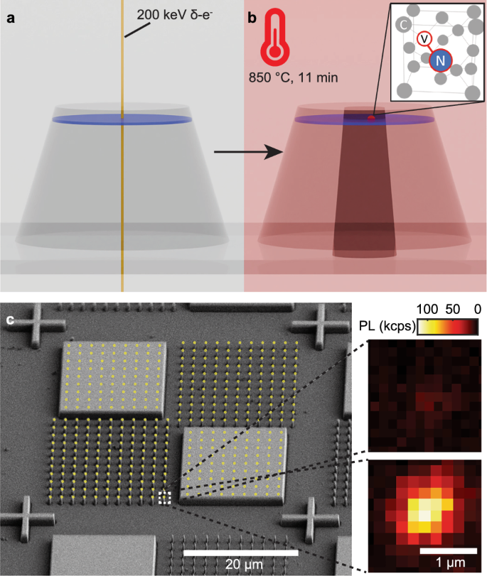
a Schematic of our formation method showing a nanopillar containing a near-surface nitrogen δ-doped layer (blue disk). In δ-electron irradiation, an electron beam of 20 nm spot size (yellow line) irradiates the center of a pillar, creating vacancies along its trajectory. b Upon annealing, monovacancies diffuse to form a vacancy-rich region (dark shaded region) in which they can be captured by nitrogen atoms to form NV centers (inset). c A scanning electron micrograph of a unit block of etched diamond pillars and mesas framed by alignment marks. Each 50 × 50 μm2 unit block consists of two unetched mesas (top left and bottom right), and two regions of nanopillars with a diameter of 280 nm (top right) and 480 nm (bottom left). The overlaid yellow circles denote the target positions of the electron beam (scale bar: 20 μm). The insets show confocal PL images of a single 480 nm pillar under 170 μW of 532 nm excitation before (top) and after (bottom) 4.8 × 10²¹ e−/cm2 δ-electron irradiation and annealing (scale bar: 1 μm).
To laterally localize NV centers, we use a commercially available 200 keV EBL tool (JBX-8100FS, JEOL Ltd.) to δ-electron irradiate the centers of the nanopillars using an electron beam of 20 nm spot size (Fig. 1a); these electrons can penetrate into the diamond and displace carbon atoms along their trajectory up to ~50 μm below the surface46,55, creating a narrow pencil of vacancies (Fig. 1a, see Supplementary Section 3). We note that 145 keV is the threshold energy for vacancy creation in diamond46 and only recently have commercial EBL tools exceeded 150 kV. The resulting monovacancy density depends on electron dose, which we tune from 1.6 × 10¹⁹ e−/cm2 to 4.8 × 10²¹ e−/cm2 by adjusting the dwell time while keeping the beam current constant at 20 nA. Subsequent annealing at 850 °C for 11 min in vacuum promotes the diffusion of monovacancies (Fig. 1b). When a monovacancy diffuses to a site adjacent to a nitrogen atom, it can get captured to form an NV center (Fig. 1b, inset). We note that NVs formed in the δ-doped N-layer can be identified by their 15NV hyperfine structure, revealed with pulsed electron spin resonance (ESR) spectroscopy. Then, the device is cleaned in a boiling nitrating acid (1:1 HNO3:H2SO4) and annealed at 450 °C in air for 4 hours. All NV measurements were taken using a home-built confocal microscope with 532 nm excitation56 (see “Methods”).
First, we show control over the number of NVs formed per nanopillar by varying the δ-electron irradiation dosage. In Fig. 2, we sweep the irradiation dose from 1.6 × 10¹⁹ e−/cm2 to 4.8 × 10²¹ e−/cm2 and measure the average number of NVs created in 280 nm (purple circles) and 480 nm (teal circles) diameter pillars. We use a maximum likelihood estimation method46 based on continuous wave-ESR spectroscopy (CW-ESR) taken on 121 pillars for each pillar size and irradiation dose after annealing (see Supplementary Section 1). With increasing irradiation dose, the average number of created NVs increases monotonically from ~5 × 10⁻² to 5.9(7) and 9.7(4) for 280 nm and 480 nm diameter pillars, respectively. We subtract the contribution from as-grown NVs, characterized by measuring non-irradiated pillars of each diameter (see Supplementary Section 1). We also estimate the average NV number per spot in δ-electron irradiated mesas by measuring the total PL around the target areas normalized by that of single NVs, as plotted in red circles in Fig. 2. Likewise, we observe a monotonic increase in the NV formation with irradiation dose.
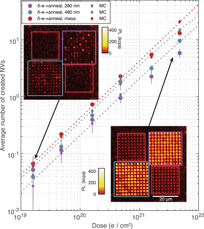
Plotted are the average number of created NVs per spot in 280 nm diameter pillars (purple circles), in 480 nm diameter pillars (teal circles), and in the mesas (red circles). The error bars denote 95% confidence interval of the NV number estimation. The results from MC simulations (diamonds) are plotted in corresponding colors and show good agreement with the measurements. The fitted curves for the MC simulation results (dotted lines) are shown as a guide to the eye. The insets show confocal micrographs of a unit block after irradiation and annealing with a dose of 1.6 × 10¹⁹ e−/cm2 (top left) and 4.8 × 10²¹ e−/cm2 (bottom right). (scale bar: 20 μm). The overlaid boxes indicate the locations of the 280 nm pillars (purple box), 480 nm pillars (teal box), and mesas (red boxes).
The increase in NV number with pillar diameter indicates that vacancies diffuse at least as far as the radius of the smaller pillar, and comparing our results to MC simulations (“Methods”) of a simple diffusion-capture model of NV formation, we extract a monovacancy diffusion constant DV = 17(4) nm2 s−1 (see Supplementary Section 5). Simulation results are plotted as diamonds in Fig. 2. At higher irradiation doses (≥1.6 × 10²¹ e−/cm2), simulations slightly overestimate NV number, which we attribute to the creation of vacancy clusters at high monovacancy density57,58,59, giving rise to sublinear monovacancy creation efficiency. In the next section, we characterize DV via an alternate approach, arriving at a similar value, and we further discuss the results.
We identify ~5 × 10²⁰ e−/cm2and 3 × 10²⁰ e−/cm2 as the target dose for an average of 1 NV per 280 nm and 480 nm pillar, respectively, facilitating the fabrication of devices based on single isolated defects for sensing and networking applications. We expect the target electron dose to vary for different nitrogen densities and nanostructure geometries.
We next demonstrate high spatial confinement of NV centers aligned to diamond nanostructures, which is necessary for optimizing spatial overlap between the defect qubit and the structure’s photonic modes. In Fig. 3, we quantify the lateral positioning precision of created NVs afforded by δ-electron irradiation. To do so, we first investigate arrays of NVs patterned in 20 × 20 μm2 mesas and quantify the deviation σloc of NV positions from their target irradiation spot. The irradiation pattern on the mesa is shown in yellow circles in Fig. 1c and example confocal images are shown in Fig. 2 (bottom right and top left square of each inset). We use these featureless mesas to avoid exciting photonic modes of the nanopillars that modify the NV emission pattern and obfuscate the actual NV position. We estimate σloc, the standard deviation of lateral NV positioning in the mesas, by pixel-wise averaging 162 tiles in the confocal image, with each 2 × 2 μm2 tile centered on a single irradiation spot; the tiles were obtained by cutting a ~40 × 40 μm2 confocal image containing two mesas (the area shown in Fig. 1c) into a regular grid (see Supplementary Section 6). Prior to this image cutting we apply global affine transformations to the original confocal image to account for optical aberrations in our imaging system. We then repeat this procedure over several different 40 × 40 μm2 confocal image areas to arrive at the pixel-wise averaged confocal images shown in the insets of Fig. 3b. Each of these images has a finite lateral spread σtot with respect to the target positions due to three contributions: the lateral NV positioning precision of our patterning technique σloc, the point spread function (PSF) of our imaging system σPSF, and residual global aberrations not removed after the first set of global affine transformations σsys:
$${\sigma }_{tot}^{2}={\sigma }_{loc}^{2}+{\sigma }_{PSF}^{2}+{\sigma }_{sys}^{2}.$$
(1)
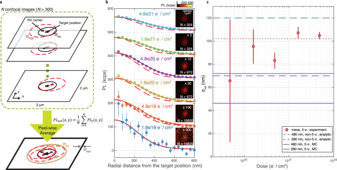
a Schematic of pixel-wise averaging method for estimating σloc. NVs are positioned at the target position (black star) with a lateral precision σloc (black solid line). Red dashed line indicates the point spread function σPSF of our confocal microscope. N confocal images of unpatterned mesas are pixel-wise averaged to give a σtot from which σloc is extracted as discussed in the main text. Residual optical aberrations are indicated by σsys. b Data points show the radial PL profiles (averaged over angle) of the pixel-wise averaged images (bin size: 40 nm). Error bars show standard error of the averaging. Colored solid lines are 2D Gaussian fits, from which σtot is extracted. For comparison, red dashed lines show the radial cuts of the 2D Gaussian functions with a peak width of \(\sqrt{{\sigma }_{PSF}^{2}+{\sigma }_{sys}^{2}}\). Plots are offset for clarity, each with a relative ΔPL of 100 kcps. Insets show the averaged images with PL scaling inversely proportional to the dose (scale bar: 1 μm). c Measured σloc in the mesas (red circles, error bar: 95% confidence interval) is plotted as a function of dose.The error bars increase at lower doses due to the smaller number of measured NVs per spot, and the 1.6 × 10¹⁹ e−/cm2 dose data point is omitted because of large errorbars >1 μm. The red dotted line indicates the average σloc of 102(2) nm measured in the mesas. Solid lines are MC simulations of \({\sigma }_{loc}^{pillar}\) in δ-e−-irradiated pillars, which are lower than the analytically calculated \({\sigma }_{loc}^{pillar}\) for NVs created without localization methods (dashed lines).
To extract σloc we first measure σtot by fitting the averaged confocal images with a 2D Gaussian curve,
$$PL(x,y)=P{L}_{max}{e}^{-({x}^{2}+{y}^{2})/(2{\sigma }_{tot}^{2})},$$
(2)
where PLmax is the maximum PL of the averaged confocal image. The radial profiles of the averaged images (circles) and the fits (solid lines) are shown in Fig. 3b. Then, we measure σPSF = 235 nm by imaging six single NVs in the mesa region and individually fitting them to a 2D Gaussian function \(P{L}_{single}(x,y)\propto {e}^{-({x}^{2}+{y}^{2})/(2{\sigma }_{PSF}^{2})}\) (see Supplementary Section 6). We characterize the residual global aberration of our transformed images to be σsys = 41 nm (see Supplementary Section 6). Finally, we extract σloc for the different irradiation dosages and plot the results in Fig. 3c (red circles). The data shows minimal dependence of σloc on dose, with an average σloc = 102(2) nm (red dotted line).
Since δ-electron irradiation creates highly localized monovacanices (see Fig. 1 and Supplementary Section 3), we attribute the majority of σloc to vacancy diffusion during annealing. Hence our measured σloc provides an estimate of DV = 21 nm2 s−1 via comparison with MC simulations (see Supplementary Section 7). This number is consistent with the estimated DV = 17(4) nm2 s−1 from NV number measurements (Fig. 2) and is within the range of values reported in the literature. We note that reported values of DV show strong sensitivity to experimental conditions including annealing temperature, annealing time, and vacancy creation method44,46,60,61,62. For instance, ref. 44 measured DV = 6.5 nm2 s−1 at 850 °C-30 min annealing and ref. 61 found DV ≤ 40 nm2 s−1 at 1050 °C-2 h annealing. Further, ref. 62 found DV can be enhanced due to transient dynamics during the first few minutes of annealing (DV ~300 nm2 s−1 for 2 min annealing at 1000 °C).
We next estimate the lateral NV positioning precision in the nanopillars \({\sigma }_{loc}^{pillar}\). We use MC simulations because a direct measurement is challenging due to the effect of the pillars’ photonic modes on the confocal images. As shown in Fig. 3c, \({\sigma }_{loc}^{pillar}\) (solid lines) is smaller than σloc, and notably smaller than \({\sigma }_{loc}^{pillar}\) for NVs uniformly distributed in a nitrogen layer bounded by the pillar walls (where \({\sigma }_{loc}^{pillar}=1/4\times\) pillar diameter), as would result from the conventional method of forming pillars after NV formation. In contrast, our technique achieves improved lateral confinement even in pillars with comparable size to σloc, a fact we attribute to vacancy absorption at the pillar sidewalls during annealing. Specifically, we find \({\sigma }_{loc}^{pillar}=46(1)\, {{{\rm{nm}}}}\) and 72(1) nm in our δ-electron irradiated 280 nm and 480 nm pillars. This improved lateral confinement is expected to enhance the coupling to the nanopillar photonic mode, as shown in the next section.
Spin and optical properties of single NVs in nanopillars
We next present the spin coherence and photoluminescence properties of single 15NV centers created inside nanopillars, confirmed by second-order correlation measurements (see Supplementary Section 8) and hyperfine-resolved pulsed ESR measurements. Figure 4a shows a histogram of the Hahn echo coherence time, \({T}_{2}^{Hahn}\), of 12 NV centers formed by 1.6 × 10²⁰ e−/cm2-irradiation. We observe reliably long \({T}_{2}^{Hahn}\) with a mean of 98(37) μs, which we attribute to the gentle nature of our NV formation process, producing little collateral damage that can adversely affect coherence. The coherence time is consistent with the limit imposed by the surrounding substitutional nitrogen (P1 center) bath(see Supplementary Section 9). In contrast, 15 keV ion implantation results in NVs with the majority ( >90%) having \({T}_{2}^{Hahn}\) less than 50 μs34. As shown in the inset, we also measure long \({T}_{2}^{Hahn}\) for single NV pillars with 4.8 × 10¹⁹ e−/cm2 irradiation, while we see a reduced \({T}_{2}^{Hahn}\) of 36(8) μs for 4.8 × 10²⁰ e−/cm2 (Fig. 4a, inset). We attribute this reduction to increased vacancy-related damage, consistent with previous reports41,60.
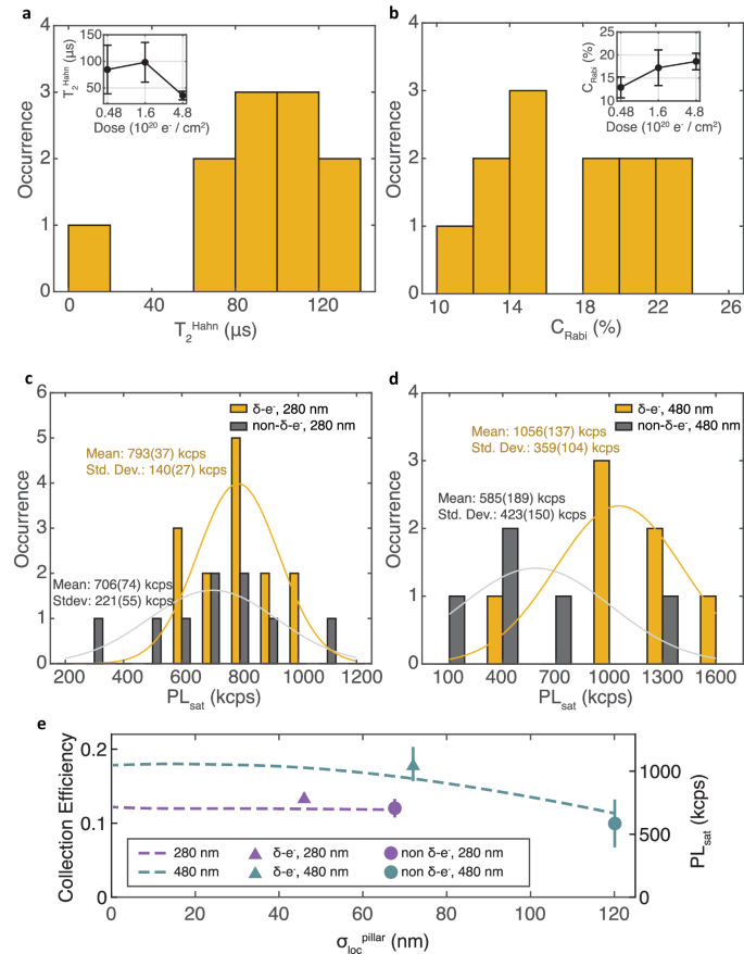
a Histogram of \({T}_{2}^{Hahn}\) for NVs δ-electron irradiated with 1.6 × 10²⁰ e−/cm2 in both 280 nm and 480 nm diameter pillars. (Inset) Average \({T}_{2}^{Hahn}\) as a function of irradiation dose. b Histogram of Rabi contrast CRabi at 1.6 × 10²⁰ e−/cm2. (Inset) Average CRabi as a function of δ-electron irradiation dose. Histogram of PLsat in c 280 nm and d 480 nm pillars. Each plot shows both non-irradiated (gray) and 1.6 × 10²⁰ e−/cm2-δ-electron irradiated (yellow) pillars. The solid curves are the Gaussian fit for the histograms. e Dashed lines indicate mean photon collection efficiency calculated from FDTD simulations for a given lateral distribution \({\sigma }_{loc}^{pillar}\). Data points are the experimentally measured sample mean of the PLsat distribution for δ-electron irradiated pillars (triangles) and non-irradiated pillars (circles) for 480 nm (teal) and 280 nm (purple) diameter pillars. The error bars denote the standard error of the estimation of the population mean. The limits of the secondary y-axis are chosen so that the simulated collection efficiency and measured PLsat for the nonirradiated pillars line up.
We also demonstrate favorable optical properties of our δ-electron irradiated single NV centers, namely good spin-dependent optical readout contrast and high photon collection rates. Figure 4b shows an average spin-dependent Rabi PL contrast \({C}_{Rabi}=\frac{P{L}_{0}-P{L}_{\pm 1}}{P{L}_{0}}\) of 18(4)% at 1.6 × 10²⁰ e−/cm2, where PL0 and PL±1 are the PL for NV electronic spin states 0 and ±1, respectively. The inset shows the dependence of CRabi on irradiation dose with no evidence of reduced contrast at the highest dosages compatible with single NV formation.
In Fig. 4c, d, we show histograms (yellow) of the saturation count rate PLsat (with background PL subtracted) for 280 nm and 480 nm pillars, respectively (see Supplementary Section 10). The means of the two PLsat histograms are 0.793(37) Mcps and 1.056(137) Mcps, respectively. Also plotted in gray are the PLsat histograms of non-irradiated pillars with as-grown single 15NVs, which have a uniform spatial distribution inside the pillars. The non-irradiated pillars show a lower mean PLsat compared to the δ-electron irradiated pillars by a factor of 1.8 and 1.1 for 480 nm and 280 nm pillars, respectively. The increase in mean PLsat in the δ-electron irradiated 480 nm pillars is statistically significant. Higher PLsat values could be achieved with pillar geometries optimized for increased collection efficiency, such as parabolic pillars63 or tapered pillars 34, where with pillars with a ~70° sidewall angle, the authors achieved an average PLsat = 1.6 Mcps.
In Fig. 4e, we conduct finite-difference time-domain (FDTD) simulations to study the effect of lateral localization on PLsat in nanopillars (see “Methods”). The simulations (dashed lines) and the data are in good agreement, indicating that increased localization precision is the main contributor to increased PLsat for the 480 nm pillars, while PLsat does not depend strongly on \({\sigma }_{loc}^{pillar}\) in the 280 nm pillars. This can be attributed to a higher-order waveguiding mode, TE01, strongly outcoupling photons from NVs close to the edge of 280 nm pillars. In contrast, for 480 nm pillars, NVs close to the edge are weakly coupled to the TE01 mode, while NVs close to the center are coupled to both the fundamental mode HE11 and the higher order mode HE12, thus exhibiting sharper PL dependence in NV lateral displacement. For both pillars, our \({\sigma }_{loc}^{pillar}\) nearly maximizes photon collection efficiency. For future applications, color center localization should be performed in conjunction with FDTD simulations to optimize the emitter overlap with the photonic mode. Overall, high collection efficiency combined with long coherence and large CRabi shown here is crucial for realizing advanced functionalities in devices for NV-based sensing, as discussed in the next section.
High-yield, scalable magnetic field sensors
Lastly, we present an outlook for the improvements our method offers to scalable, high-yield fabrication of highly sensitive magnetic field sensors.
In a typical optical spin-state readout scheme, the alternating current (AC) magnetic field sensitivity η is given as
$$\eta=\frac{\hslash }{{g}_{e}{\mu }_{B}}\frac{1}{{e}^{(-2\tau /{T}_{2}^{Hahn})}\sqrt{2\tau }}\sqrt{1+\frac{4}{{C}_{Rabi}^{2}{n}_{{{{\rm{avg}}}}}}},$$
(3)
where ℏ is the reduced Planck constant, ge ≈ 2 is the NV’s electronic g factor, μB is the Bohr magneton, 2τ is the total free evolution time, and navg is the average photon number per measurement. This expression highlights the importance of long \({T}_{2}^{Hahn}\), large CRabi, and high PL for sensing small magnetic fields.
Figure 5a shows simulated histograms of η for NVs in pillars formed via our method (yellow) compared to two other methods: conventional 30 keV nitrogen-implanted layers (cyan) and δ-doped layers without lateral localization (gray). Also plotted are δ-electron irradiated pillars with future improvements to the pillar geometry (green). The distributions are generated using Equation (3) with navg = 0.5 ⋅ PLsat ⋅ 400 ns and \(2\tau={T}_{2}^{Hahn}\) with the PLsat, CRabi and \({T}_{2}^{Hahn}\) distributions experimentally measured in this work. From this histogram, we calculate the cumulative density function P(X < η) for the corresponding sensitivity distribution X in Fig. 5b. The median η of NVs formed using our method is \(42\,{{{\rm{nT}}}}/\sqrt{{{{\rm{Hz}}}}}\) with 86% of the NV centers exhibiting \(\eta \lesssim 68\,{{{\rm{nT}}}}/\sqrt{{{{\rm{Hz}}}}}\). For reference, a 53-nm deep NV with \(\eta=68\,{{{\rm{nT}}}}/\sqrt{{{{\rm{Hz}}}}}\) can detect a single electron spin at the diamond surface in a typical averaging time of 1 minute43. For the non-localized δ-doped method, the median η is \(63\,{{{\rm{nT}}}}/\sqrt{{{{\rm{Hz}}}}}\) with 57% of the NVs exhibiting \(\eta \lesssim 68\,{{{\rm{nT}}}}/\sqrt{{{{\rm{Hz}}}}}\), where we use the measured PLsat, CRabi, and \({T}_{2}^{Hahn}\) distributions of non-irradiated pillars. With the conventional, implantation-based method, the median η is \(121\,{{{\rm{nT}}}}/\sqrt{{{{\rm{Hz}}}}}\) with 29% of the NVs exhibiting \(\eta \lesssim 68\,{{{\rm{nT}}}}/\sqrt{{{{\rm{Hz}}}}}\), where we use the measured PLsat and CRabi distributions from non-irradiated pillars with the reported distribution of \({T}_{2}^{Hahn}\) from 30 keV implantation64, chosen because it produces a similar NV depth of 40–50 nm. Hence, our method produces a significantly higher yield of high-sensitivity NV magnetometers, where we demonstrate an estimated 3-fold higher yield of single-electron-spin detectable magnetometers compared to conventional implantation-based methods. We note that further improvements can be realized by utilizing pillars with a 70° sidewall taper angle34, as shown in green in Fig. 5. Higher-order dynamical decoupling can also extend coherence time, where an order of magnitude increase for shallow, δ-doped NVs has been demonstrated47, leading to a further 3× improvement in η to \( < 10\,{{{\rm{nT}}}}/\sqrt{{{{\rm{Hz}}}}}\). For comparison, the reported values of η of single NV magnetometers for nanoscale imaging include \(56\,{{{\rm{nT}}}}/\sqrt{{{{\rm{Hz}}}}}\)65, \(56\,{{{\rm{nT}}}}/\sqrt{{{{\rm{Hz}}}}}\) (dynamical decoupling with 512-pulse XY8: \(18\,{{{\rm{nT}}}}/\sqrt{{{{\rm{Hz}}}}}\))66, \(104\,{{{\rm{nT}}}}/\sqrt{{{{\rm{Hz}}}}}\)67, and \(66\,{{{\rm{nT}}}}/\sqrt{{{{\rm{Hz}}}}}\) (dynamical decoupling with 128-pulse XY8: \(32\,{{{\rm{nT}}}}/\sqrt{{{{\rm{Hz}}}}}\))68.
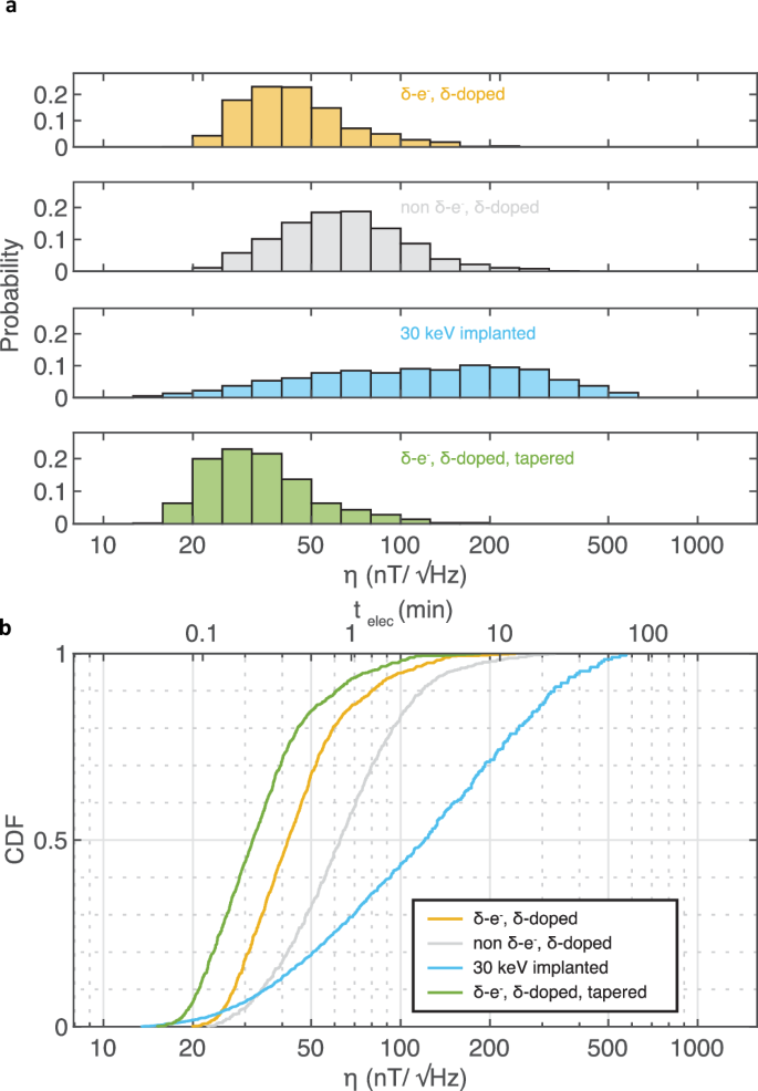
a Histogram and b cumulative density function (CDF) of the estimated AC magnetic field sensitivity η of single NVs in 480 nm pillars. The η distribution is estimated for δ-doped, δ-electron irradiated (yellow) and δ-doped, non-irradiated (gray) pillars using measured PLsat, \({T}_{2}^{Hahn}\) and CRabi distributions. The η distribution of conventionally implanted pillars (cyan) is generated using PLsat and CRabi measurements on our non-irradiated pillars with reported \({T}_{2}^{Hahn}\) distribution for 30 keV implantation64. The distribution for δ-doped, δ-electron irradiated pillar with better sidewall taper angle of 70∘ (green) is also estimated using \({T}_{2}^{Hahn}\) and CRabi measurements on our δ-electron irradiated pillars with the estimated PL improvement from FDTD simulations. A secondary x-axis shows the minimum averaging time for a 53 nm-deep NV to detect a single electron spin located on the diamond surface.
Discussion
To conclude, we demonstrate three-dimensionally localized formation of highly coherent NV centers aligned to prefabricated nanophotonic structures. Using our method, we find NV spin and photoluminescence properties superior to those for NV centers formed via conventional implantation methods as well as nonlocalized δ-doped methods. These improved properties culminate in a significantly higher yield of high-sensitivity magnetometers, an important application of NV centers. Through our work, we also gain an understanding of vacancy diffusion in nanostructured diamond devices.
While we demonstrate our technique here on NV centers in diamond nanopillars, we emphasize that our method can be readily applied to other device geometries, such as 2D and 1D photonic crystal cavities24,33 and nano-optomechanical devices69 as well as to other material systems, including divacancies70 and silicon vacancies71 in silicon carbide and T centers in silicon72. In these optically addressable qubit systems, the advantages outlined here can be transferred using a similar targeted irradiation technique guided by our model of vacancy diffusion and capture for different geometries. The versatility of our method makes it attractive to apply to, for instance, NV center formation in (111)-oriented diamonds42, with prospects of improved photon count rates in nanopillars73, circular “bulls-eye" cavities for enhanced photon collection74, as well as shallow (<~10 nm deep) NV centers, with applications in NV-driven magnetic resonance imaging and ultra-high spatial resolution imaging of condensed matter systems.
Looking forward, there is still room for further improvement in the collective control over the number, position, and coherence of color centers. The ultimate goal of forming a single defect with unit probability at a spot can be achieved by, for instance, δ-electron irradiation with in-situ annealing and photoluminescence characterization51. Lateral confinement can be enhanced by reducing the annealing time tanneal, i.e., \({\sigma }_{loc}\propto {t}_{anneal}^{0.5}\), though the tradeoffs with potentially reduced coherence and NV yield will need to be optimized45. Reducing the nitrogen density within the δ-doped layer is expected to extend \({T}_{2}^{Hahn}\) beyond 1 ms46, and again, the tradeoff with NV number will need to be explored. Overall, our results strengthen the role of optically addressable solid-state spin defects in next-generation metrology and information science.
Methods
PECVD diamond growth
Diamond homoepitaxial growth and δ-doping were performed via plasma-enhanced chemical vapor deposition (PECVD) using a SEKI SDS6300 reactor on a (100) oriented electronic grade diamond substrate (Element Six Ltd.). Prior to growth, the substrate was fine-polished by Syntek Ltd. to a surface roughness of ~200–300 pm, followed by a 4–5 μm etch to relieve polishing-induced strain. The growth conditions consisted of a 750 W plasma containing 0.1% 12CH4 in 400 sccm H2 flow held at 25 torr and ~730 °C according to a pyrometer. A ~154 nm-thick isotopically purified (99.998% 12C) epilayer was grown. During the nitrogen δ-doping period of growth, 15N2 gas 1.0% of the total gas content) is introduced into the chamber for five minutes. After growth, the sample was characterized with secondary ion mass spectrometry (SIMS) to estimate the isotopic purity, epilayer thickness, and properties of the δ-doped layer (3.6 nm thick, 98 ppm nm, see Supplementary Section 2).
NV characterization
All NV measurements are performed using a home-built confocal microscope using a 532 nm laser in an external magnetic field of 50–100 G. A 0.7 NA objective lens collects the emitted photons, which are then filtered 594 nm by a long-pass filter (SEMROCK BLP01-594R-25) and detected using an avalanche photodiode (SPCM-AQRH-14-FC). Microwave signals are delivered through an external gold wire.
Monte Carlo simulations
We simulate NV center formation using MC simulation. Our simulation models the dominant effects during the annealing step, namely the diffusion of monovacancies within the prefabricated device and their capture by the existing nitrogen atoms to form NV centers. We also consider vacancy recombination at the diamond surfaces39,75 (e.g., the top surface and the pillar’s sidewalls for nanopillars).
Simulating the atomic-scale diffusion process on a diamond lattice is computationally intensive, necessitating approximately 50 million discrete “jumps” for a vacancy to traverse 1 μm, with each jump spanning a minuscule 0.154 nm C–C bond spacing. Therefore, we adopt a coarse-grained approach with a cubic lattice of spacing 1 nm, still significantly smaller than the device dimensions. Within each simulation run, we randomly select positions for NN nitrogen atoms within the δ-doped layer region and NV vacancies within the vacancy-rich area from 200 keV electron irradiation. We estimate NV from CASINO simulations with a scaling factor α, which is set as a free parameter (see Supplementary Section 4). For computational efficiency, we only consider vacancies with depth (<1 μm) since deeper vacancies do not contribute to NV center formation.
Given the initial conditions of the simulations, we segment the annealing process into shorter time steps. In each step, all vacancies randomly move some number of jumps, after which we check if they encountered a capture event. A capture by a nitrogen atom can occur when a monovacancy is in the same coarse-grained cell as a nitrogen atom with a probability of \(\frac{16{V}_{cc}/{V}_{uc}}{{(8{V}_{cc}/{V}_{uc})}^{2}/2}\), where Vcc and Vuc are the volumes of the coarse-grained cell and unit cell, respectively. When an NV center forms, both the vacancy and the nitrogen atom are removed from the simulation during the subsequent time steps. Conversely, if a monovacancy gets captured by the boundaries, only the vacancy is eliminated.
Finite-difference time-domain simulations
Ansys Lumerical FDTD software is used to simulate the collection efficiency of photons emitted by NVs inside nanopillars. We model an NV as a point source consisting of two orthogonal dipoles perpendicular to the NV axis. The emission frequency range of the dipole is chosen to match the frequency range of the phonon sideband of the NV emission spectrum at room temperature: 650–800 nm. The NVs are positioned 53 nm below the top surface. We simulate our two nanopillar geometries with diameters 280 nm and 480 nm with the side wall angle of ~83° and height of 1.4 μm, which are attached to a diamond slab of finite thickness. For computational efficiency, we set the thickness of the slab to be 1 μm. To avoid any interference due to this relatively thin slab, we absorb all incoming fields at the bottom surface of the slab. We do this by setting the simulation area such that the bottom diamond interface matches the perfectly absorbing simulation boundary. The collection efficiency is then calculated from the power transmitted to a monitor plane just below the pillar inside the slab. We calculate the far-field emission through a collection cone with NA = 0.7.
To calculate the mean collection efficiency for the distribution of NVs with a given \({\sigma }_{loc}^{pillar}\), we first sweep the position of the NV laterally in two orthogonal directions (dx and dy) and calculate the collection efficiency. Then, we extrapolate the collection efficiency for a given radial displacement \(\overrightarrow{dr}=(dr\cos \theta,dr\sin \theta )\) by assuming the superposition of two orthogonal NVs. In particular, the collection efficiency is calculated as a weighted average of those calculated at two orthogonal displacements dx = dr and dy = dr, where the weights are given as \({\cos }^{2}\theta\) and \({\sin }^{2}\theta\), respectively. We sweep the lateral confinement of NVs from perfectly localized (\({\sigma }_{loc}^{pillar}=0{{{\rm{nm}}}}\)) to maximally delocalized (\({\sigma }_{loc}^{pillar}=1/4\times\) pillar diameter, corresponding to a uniform lateral distribution across the pillar). For simplicity, we set the lateral probability distribution to follow a 2D Gaussian function with a spread of σ0 which we truncate at the pillar boundary beyond which the probability is zero. For a given σ0, we use the probability distribution and simulated collection efficiency to calculate both \({\sigma }_{loc}^{pillar}\) and the mean of the collection efficiency.
Data availability
All the experimental data used in this work are available via Zenodo at https://doi.org/10.5281/zenodo.16747927.
References
Awschalom, D. D., Hanson, R., Wrachtrup, J. & Zhou, B. B. Quantum technologies with optically interfaced solid-state spins. Nat. Photonics 12, 516–527 (2018).
Wolfowicz, G. et al. Quantum guidelines for solid-state spin defects. Nat. Rev. Mater. 6, 906–925 (2021).
Doherty, M. W. et al. The nitrogen-vacancy colour centre in diamond. Phys. Rep. 528, 1–45 (2013).
Yale, C. G. et al. All-optical control of a solid-state spin using coherent dark states. Proc. Natl. Acad. Sci. USA 110, 7595–7600 (2013).
Hilser, F. & Burkard, G. All-optical control of the spin state in the NV-center in diamond. Phys. Rev. B 86, 125204 (2012).
Bernien, H. et al. Heralded entanglement between solid-state qubits separated by three metres. Nature 497, 86–90 (2013).
Stolk, A. J. et al. Metropolitan-scale heralded entanglement of solid-state qubits. Sci. Adv. 10, eadp6442 (2024).
Tomljenovic-Hanic, S., Steel, M. J., Sterke, C. M. D. & Salzman, J. Diamond based photonic crystal microcavities. Opt. Express 14, 3556–3562 (2006).
Lukin, D. M. et al. 4H-silicon-carbide-on-insulator for integrated quantum and nonlinear photonics. Nat. Photonics 14, 330–334 (2020).
Babin, C. et al. Fabrication and nanophotonic waveguide integration of silicon carbide colour centres with preserved spin-optical coherence. Nat. Mater. 21, 67–73 (2022).
Bhaskar, M. K. et al. Experimental demonstration of memory-enhanced quantum communication. Nature 580, 60–64 (2020).
Stas, P.-J. et al. Robust multi-qubit quantum network node with integrated error detection. Science 378, 557–560 (2022).
Wang, C. F. et al. Fabrication and characterization of two-dimensional photonic crystal microcavities in nanocrystalline diamond. Appl. Phys. Lett. 91, 201112 (2007).
Marseglia, L. et al. Nanofabricated solid immersion lenses registered to single emitters in diamond. Appl. Phys. Lett. 98, 133107 (2011).
Huang, T.-Y. et al. A monolithic immersion metalens for imaging solid-state quantum emitters. Nat. Commun. 10, 2392 (2019).
Khanaliloo, B. et al. Single-crystal diamond nanobeam waveguide optomechanics. Phys. Rev. X 5, 041051 (2015).
Zhou, T. X., Stöhr, R. J. & Yacoby, A. Scanning diamond NV center probes compatible with conventional AFM technology. Appl. Phys. Lett. 111, 163106 (2017).
Babinec, T. M. et al. A diamond nanowire single-photon source. Nat. Nanotechnol. 5, 195–199 (2010).
Jamali, M. et al. Microscopic diamond solid-immersion-lenses fabricated around single defect centers by focused ion beam milling. Rev. Sci. Instrum. 85, 123703 (2014).
Gadalla, M. N., Greenspon, A. S., Defo, R. K., Zhang, X. & Hu, E. L. Enhanced cavity coupling to silicon vacancies in 4H silicon carbide using laser irradiation and thermal annealing. Proc. Natl. Acad. Sci. USA 118, e2021768118 (2021).
Crook, A. L. et al. Purcell enhancement of a single silicon carbide color center with coherent spin control. Nano Lett. 20, 3427–3434 (2020).
Bracher, D. O., Zhang, X. & Hu, E. L. Selective Purcell enhancement of two closely linked zero-phonon transitions of a silicon carbide color center. Proc. Natl. Acad. Sci. USA 114, 4060–4065 (2017).
Faraon, A., Santori, C., Huang, Z., Acosta, V. M. & Beausoleil, R. G. Coupling of nitrogen-vacancy centers to photonic crystal cavities in monocrystalline diamond. Phys. Rev. Lett. 109, 033604 (2012).
Hausmann, B. J. M. et al. Coupling of NV centers to photonic crystal nanobeams in diamond. Nano Lett. 13, 5791–5796 (2013).
Riedrich-Möller, J. et al. Nanoimplantation and Purcell enhancement of single nitrogen-vacancy centers in photonic crystal cavities in diamond. Appl. Phys. Lett. 106, 221103 (2015).
Zhang, Q. et al. High-fidelity single-shot readout of single electron spin in diamond with spin-to-charge conversion. Nat. Commun. 12, 1529 (2021).
Evans, R. E. et al. Photon-mediated interactions between quantum emitters in a diamond nanocavity. Science 362, 662–665 (2018).
Pingault, B. et al. All-optical formation of coherent dark states of silicon-vacancy spins in diamond. Phys. Rev. Lett. 113, 263601 (2014).
Becker, J. N., Görlitz, J., Arend, C., Markham, M. & Becher, C. Ultrafast all-optical coherent control of single silicon vacancy colour centres in diamond. Nat. Commun. 7, 13512 (2016).
Cui, S. et al. Reduced plasma-induced damage to near-surface nitrogen-vacancy centers in diamond. Nano Lett. 15, 2887–2891 (2015).
Lesik, M. et al. Maskless and targeted creation of arrays of colour centres in diamond using focused ion beam technology. Phys. Status Solidi 210, 2055–2059 (2013).
Pezzagna, S. et al. Nanoscale engineering and optical addressing of single spins in diamond. Small 6, 2117–2121 (2010).
Schröder, T. et al. Scalable fabrication of coupled NV center-photonic crystal cavity systems by self-aligned N ion implantation. Opt. Mater. Express 7, 1514–1524 (2017).
Wang, M. et al. Self-aligned patterning technique for fabricating high-performance diamond sensor arrays with nanoscale precision. Sci. Adv. 8, eabn9573 (2022).
Van Dam, S. B. et al. Optical coherence of diamond nitrogen-vacancy centers formed by ion implantation and annealing. Phys. Rev. B 99, 161203 (2019).
Kasperczyk, M. et al. Statistically modeling optical linewidths of nitrogen vacancy centers in microstructures. Phys. Rev. B 102, 075312 (2020).
Momenzadeh, S. A. et al. Nanoengineered diamond waveguide as a robust bright platform for nanomagnetometry using shallow nitrogen vacancy centers. Nano Lett. 15, 165–169 (2015).
Tetienne, J.-P. et al. Spin properties of dense near-surface ensembles of nitrogen-vacancy centers in diamond. Phys. Rev. B 97, 085402 (2018).
Pezzagna, S., Naydenov, B., Jelezko, F., Wrachtrup, J. & Meijer, J. Creation efficiency of nitrogen-vacancy centres in diamond. N. J. Phys. 12, 065017 (2010).
Toyli, D. M., Weis, C. D., Fuchs, G. D., Schenkel, T. & Awschalom, D. D. Chip-scale nanofabrication of single spins and spin arrays in diamond. Nano Lett. 10, 3168–3172 (2010).
Hughes, L. B. et al. Two-dimensional spin systems in PECVD-grown diamond with tunable density and long coherence for enhanced quantum sensing and simulation. APL Mater. 11, 021101 (2023).
Hughes, L. B. et al. Strongly interacting, two-dimensional, dipolar spin ensembles in (111)-oriented diamond. Phys. Rev. X 15, 021035 (2025).
Ohno, K. et al. Engineering shallow spins in diamond with nitrogen delta-doping. Appl. Phys. Lett. 101, 082413 (2012).
Ohno, K. et al. Three-dimensional localization of spins in diamond using 12C implantation. Appl. Phys. Lett. 105, 052406 (2014).
Eichhorn, T. R., McLellan, C. A. & Bleszynski Jayich, A. C. Optimizing the formation of depth-confined nitrogen vacancy center spin ensembles in diamond for quantum sensing. Phys. Rev. Mater. 3, 113802 (2019).
McLellan, C. A. et al. Patterned formation of highly coherent nitrogen-vacancy centers using a focused electron irradiation technique. Nano Lett. 16, 2450–2454 (2016).
Myers, B. et al. Probing surface noise with depth-calibrated spins in diamond. Phys. Rev. Lett. 113, 027602 (2014).
Lee, J. C. et al. Deterministic coupling of delta-doped nitrogen vacancy centers to a nanobeam photonic crystal cavity. Appl. Phys. Lett. 105, 261101 (2014).
Chen, Y.-C. et al. Laser writing of coherent colour centres in diamond. Nat. Photonics 11, 77–80 (2017).
Kurita, T. et al. Efficient generation of nitrogen-vacancy center inside diamond with shortening of laser pulse duration. Appl. Phys. Lett. 113, 211102 (2018).
Chen, Y.-C. et al. Laser writing of individual nitrogen-vacancy defects in diamond with near-unity yield. Optica 6, 662–667 (2019).
Stephen, C. J. et al. Deep three-dimensional solid-state qubit arrays with long-lived spin coherence. Phys. Rev. Appl. 12, 064005 (2019).
Fujiwara, M. et al. Creation of NV centers over a millimeter-sized region by intense single-shot ultrashort laser irradiation. APL Photonics 8, 036108 (2023).
Shimotsuma, Y. et al. Formation of NV centers in diamond by a femtosecond laser single pulse. Opt. Express 31, 1594–1603 (2023).
Campbell, B. & Mainwood, A. Radiation damage of diamond by electron and gamma irradiation. Phys. Status Solidi 181, 99–107 (2000).
Bluvstein, D., Zhang, Z. & Jayich, A. C. B. Identifying and mitigating charge instabilities in shallow diamond nitrogen-vacancy centers. Phys. Rev. Lett. 122, 076101 (2019).
Iakoubovskii, K. & Stesmans, A. Vacancy clusters in diamond studied by electron spin resonance. Phys. Status Solidi 201, 2509–2515 (2004).
Davies, G., Lawson, S. C., Collins, A. T., Mainwood, A. & Sharp, S. J. Vacancy-related centers in diamond. Phys. Rev. B 46, 13157–13170 (1992).
Santonocito, S. et al. NV centres by vacancies trapping in irradiated diamond: experiments and modelling. N. J. Phys. 26, 013054 (2024).
Alsid, S. T. et al. Photoluminescence decomposition analysis: a technique to characterize N-V creation in diamond. Phys. Rev. Appl. 12, 044003 (2019).
Acosta, V. M. et al. Diamonds with a high density of nitrogen-vacancy centers for magnetometry applications. Phys. Rev. B 80, 115202 (2009).
Onoda, S. et al. Diffusion of vacancies created by high-energy heavy ion strike into diamond. Phys. Status Solidi 214, 1700160 (2017).
Hedrich, N., Rohner, D., Batzer, M., Maletinsky, P. & Shields, B. J. Parabolic diamond scanning probes for single-spin magnetic field imaging. Phys. Rev. Appl. 14, 064007 (2020).
Jakobi, I. et al. Efficient creation of dipolar coupled nitrogen-vacancy spin qubits in diamond. J. Phys. 752, 012001 (2016).
Maletinsky, P. et al. A robust scanning diamond sensor for nanoscale imaging with single nitrogen-vacancy centres. Nat. Nanotechnol. 7, 320–324 (2012).
Grinolds, M. S. et al. Nanoscale magnetic imaging of a single electron spin under ambient conditions. Nat. Phys. 9, 215–219 (2013).
Vool, U. et al. Imaging phonon-mediated hydrodynamic flow in WTe2. Nat. Phys. 17, 1216–1220 (2021).
Palm, M. et al. Imaging of submicroampere currents in bilayer graphene using a scanning diamond magnetometer. Phys. Rev. Appl. 17, 054008 (2022).
Cady, J. V. et al. Diamond optomechanical crystals with embedded nitrogen-vacancy centers. Quantum Sci. Technol. 4, 024009 (2019).
Christle, D. J. et al. Isolated electron spins in silicon carbide with millisecond coherence times. Nat. Mater. 14, 160–163 (2015).
Widmann, M. et al. Coherent control of single spins in silicon carbide at room temperature. Nat. Mater. 14, 164–168 (2015).
MacQuarrie, E. et al. Generating T centres in photonic silicon-on-insulator material by ion implantation. New J. Phys. 23, 103008 (2021).
Neu, E. et al. Photonic nano-structures on (111)-oriented diamond. Appl. Phys. Lett. 104, 153108 (2014).
Li, L. et al. Efficient photon collection from a nitrogen vacancy center in a circular bullseye grating. Nano Lett. 15, 1493–1497 (2015).
Räcke, P., Pietzonka, L., Meijer, J., Spemann, D. & Wunderlich, R. Vacancy diffusion and nitrogen-vacancy center formation near the diamond surface. Appl. Phys. Lett. 118, 204003 (2021).
Acknowledgements
The authors thank Hitoshi Kato and JEOL Ltd. for 200 keV electron irradiation. We gratefully acknowledge the support of the Gordon and Betty Moore Foundation’s EPiQS Initiative via Grant GBMF10279. We also acknowledge support from Cooperative Research on Quantum Technology (2022M3K4A1094777) through the National Research Foundation of Korea(NRF) funded by the Korean government (Ministry of Science and ICT(MSIT)), and from the DOE Q-NEXT Center (Grant No. DOE 1F-60579). The authors acknowledge the use of shared facilities of the UCSB Quantum Foundry through Q-AMASE-i program (NSF DMR1906325), the UCSB MRSEC (NSF DMR 1720256), the UCSB Nanofabrication Facility (an open access laboratory), and the Quantum Structures Facility within the UCSB California NanoSystems Institute. S.A.M acknowledges support from UCSB Quantum Foundry. L.B.H. acknowledges support from the NSF Graduate Research Fellowship Program (DGE 2139319) and the UCSB Quantum Foundry.
Ethics declarations
Competing interests
The authors declare no competing interests.
Peer review
Peer review information
Nature Communications thanks Madelaine Liddy, Fang-Wen Sun, Junfeng Wang, and the other anonymous reviewer for their contribution to the peer review of this work. A peer review file is available.
Additional information
Publisher’s note Springer Nature remains neutral with regard to jurisdictional claims in published maps and institutional affiliations.
Supplementary information
Rights and permissions
Open Access This article is licensed under a Creative Commons Attribution 4.0 International License, which permits use, sharing, adaptation, distribution and reproduction in any medium or format, as long as you give appropriate credit to the original author(s) and the source, provide a link to the Creative Commons licence, and indicate if changes were made. The images or other third party material in this article are included in the article's Creative Commons licence, unless indicated otherwise in a credit line to the material. If material is not included in the article's Creative Commons licence and your intended use is not permitted by statutory regulation or exceeds the permitted use, you will need to obtain permission directly from the copyright holder. To view a copy of this licence, visit http://creativecommons.org/licenses/by/4.0/.
About this article
Cite this article
Kim, S., London, P., Yang, D. et al. Scalable nanoscale positioning of highly coherent color centers in prefabricated diamond nanostructures. Nat Commun 16, 9803 (2025). https://doi.org/10.1038/s41467-025-64758-4
Received: 30 January 2025
Accepted: 24 September 2025
Published: 06 November 2025
Version of record: 06 November 2025
DOI: https://doi.org/10.1038/s41467-025-64758-4

