.png)

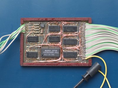 One of [NE555]’s boards from the 90s.
Back in the 90s when surface mount components gained widespread adoption, the quick and cheap PCB prototyping services of today were unavailable. This led many to develop their own approaches. In Japan a particularly novel and beautiful approach was, and still is, somewhat popular. [NE555]’s work is a excellent example of this technique using a fine enameled wire (you can find this on eBay as “magnet wire”), wirewrap board, and careful hand soldering. [NE555] has made a great video on the process (which you can watch below).
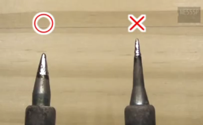 [NE555] uses a slightly fatter, stumpier tip. This likely works well due to it’s increased heat capacity.
In [NE555]’s video a relatively large tip is used. The ICs legs are pre-tinned, and the IC is glued to the board, with Polyimide (Kapton) tape insulating the legs. [NE555] uses a self-developed wirewrap pen as an aid when connecting pins. There are some details of this process in English available. Aside from this, fairly standard tools are used. The fact that [NE555] uses quality Hozan brand wire cutters likely helps with the precision wire trimming required.
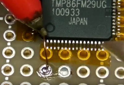 Soldering in progress
What’s quite shocking for me, is the [NE555] uses no optical aids. Most of my own SMD rework take place under an inspection microscope, but clearly [NE555]’s years of experience allow the process to be completed by eye. A microscope however is used for final inspection. While techniques like these maybe slowly replaced I can’t help but admire the craftsmanship and tenacity required to construct these beautiful prototypes. For more examples of these wonderful boards, check out the pictures and video below (and follow NE555 on twitter!)
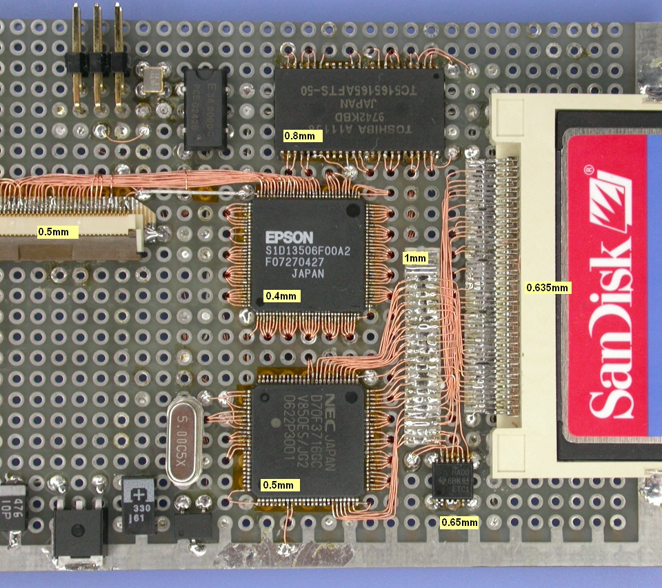 Another beautifully constructed board.