.png)

Over the past century, we’ve made tremendous advances in protecting against water-borne, food-borne, and vector-borne diseases, but the air we share remains our biggest vulnerability. Airborne infectious diseases cost millions of lives, from the estimated 27 million killed by COVID-19 to the 1.6 million who die from tuberculosis annually. As the risk of engineered pandemics and biological weapons continues to increase, experts now estimate there is a 1 in 8 chance of a pandemic killing over 90 million people by 2050.
Far-UVC light offers a new line of defence, promising to make the air we breathe as safe as the water we drink.
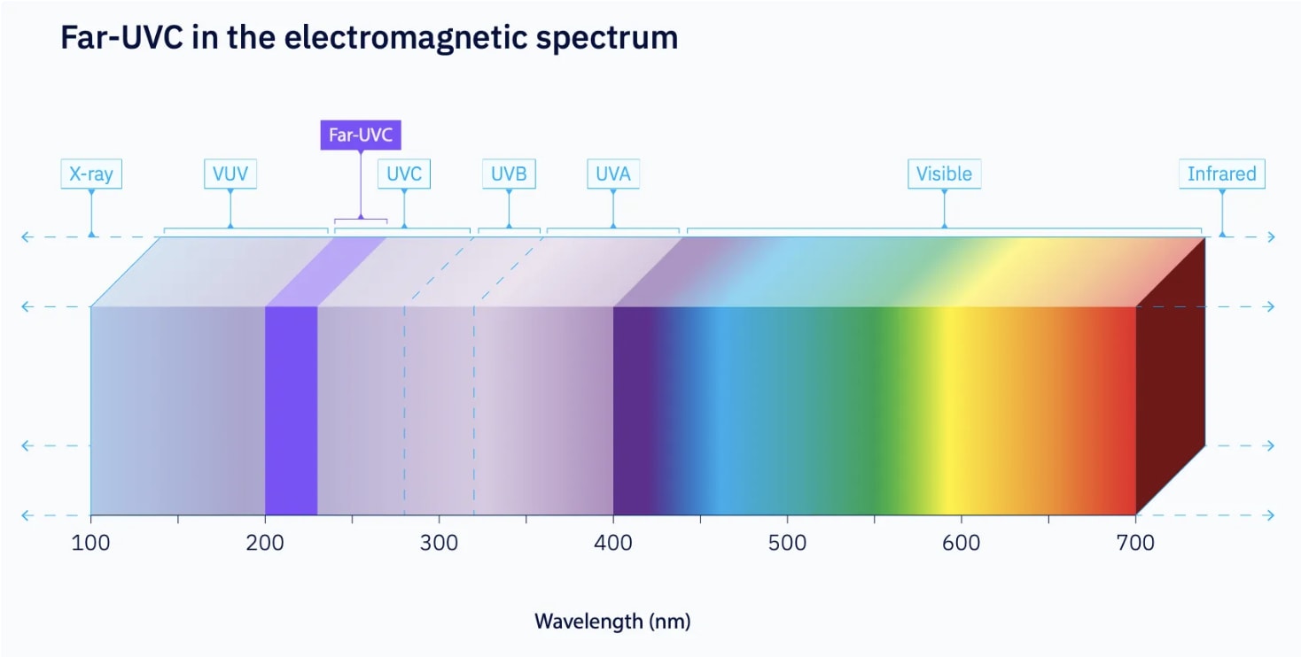
Far-UVC is a specific range of ultraviolet-C radiation, typically between 200 to 230 nanometers (nm), that has garnered significant attention for its ability to effectively neutralise pathogens while being safe for human exposure in occupied spaces. This technology holds the potential to revolutionise disinfection in healthcare, public transportation, and various other settings.
So why is this seemingly perfect technology implemented everywhere? Well, one of the main bottlenecks is the production of the light source itself.
This article explores that central challenge and its potential solutions. We will cover:
The Fundamentals: An overview of how far-UVC inactivates pathogens without harming people and why I believe it’s a worthwhile investment over other germicidal solutions.
The Bottleneck to Adoption: An analysis of one of the primary barriers to widespread adoption: the high cost, inefficiency, and practical limitations of current Far-UVC light sources.
Far-UVC LED and the History of the Blue LED: Why a direct far-UVC LED could be the key to unlocking this technology, and what we can learn from the Nobel Prize-winning breakthrough of the blue LED.
The Future: A look at how AI could accelerate development.
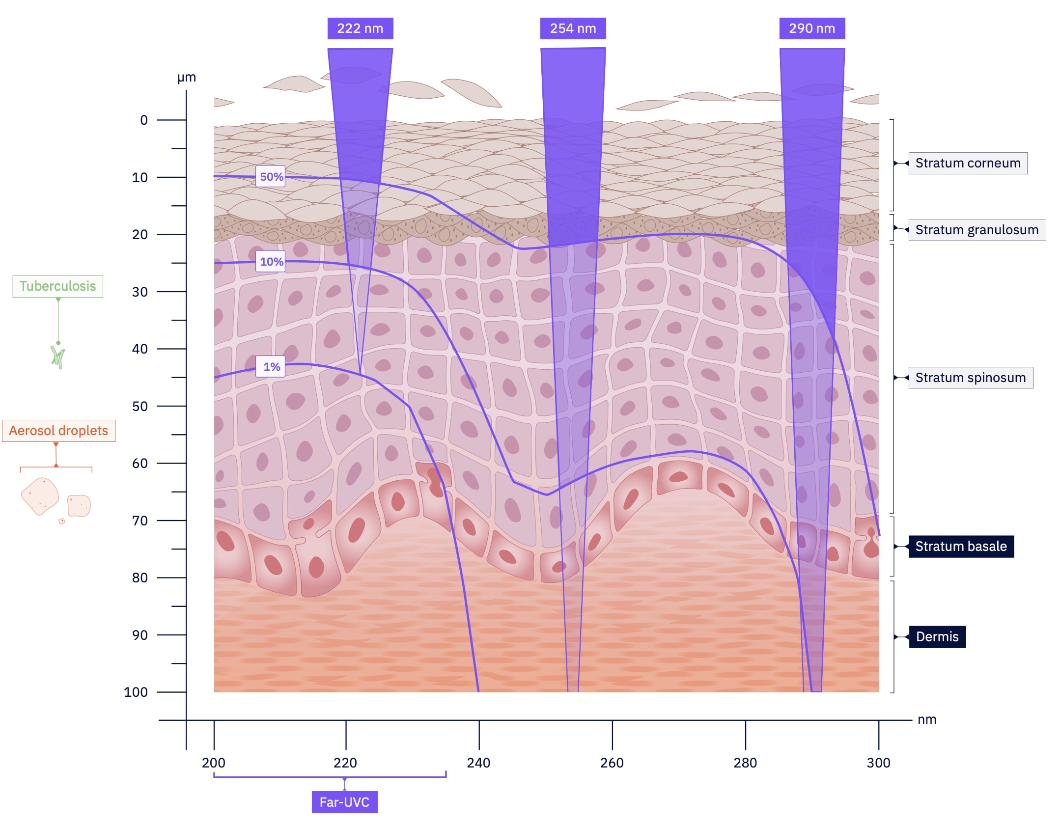
The germicidal properties of ultraviolet light have been known for over a century. Conventional UVC light, usually at a wavelength of 254 nm, is highly effective at killing microbes by damaging their DNA and RNA. However, this wavelength is also harmful to human skin and eyes, limiting its use to unoccupied spaces or within enclosed systems.
Far-UVC light, in contrast, has a much shorter wavelength. This shorter wavelength means it is strongly absorbed by biological materials, meaning its penetration is limited to the non-living outer layer of the skin and the very top of the eye’s surface. While safety studies are ongoing [1][2][3], this is why far-UVC is widely regarded as safe for use in the presence of people.
Pathogens such as viruses and bacteria are significantly smaller than human cells. This minuscule size allows the far-UVC light to penetrate and inactivate them effectively. The light disrupts their genetic material, rendering them unable to replicate and cause infection. This unique combination of potent germicidal action and human safety is the cornerstone of far-UVC technology’s potential.
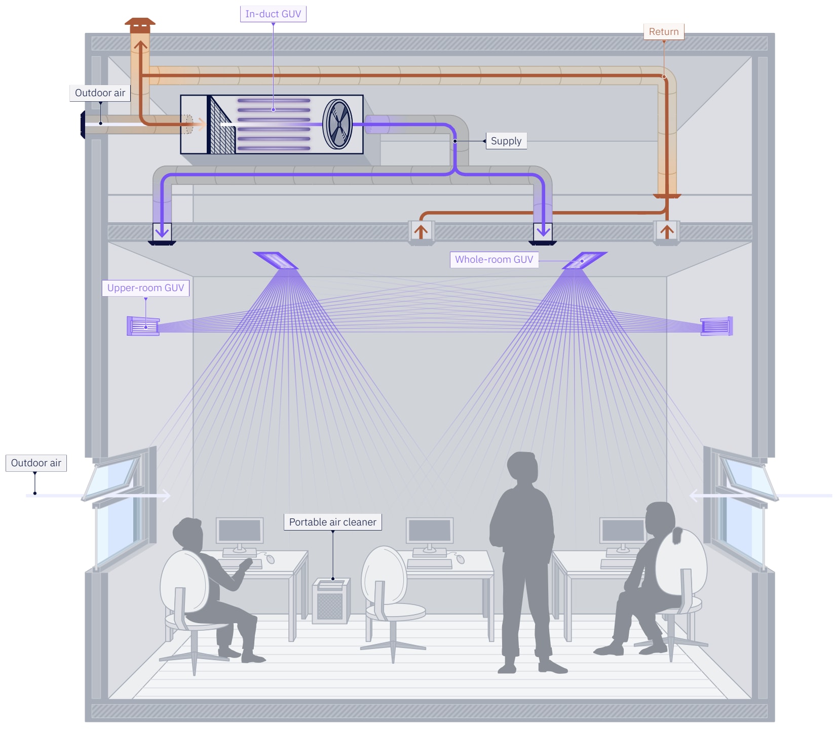
Right now, we mainly try to clean indoor air with either UV lights pointed at the ceiling or with big HEPA filter units. Both of these have major drawbacks, they only clean the air far away from people and rely on sufficient air circulation to do their job. On top of that, they can be very expensive to install and maintain.
The properties of Far-UVC overcome these exact problems. It works directly on the air between people, neutralising germs right at the source. Plus, its effectiveness doesn’t depend on perfect air circulation, and it can even be fitted into existing light fixtures for a much simpler solution.
The goal isn’t to necessarily replace our current methods, but to enhance them. For a truly comprehensive defence against airborne diseases, we need to layer them with the germicidal technology of Far-UVC.
The economic argument for having far-UVC in public spaces is also compelling. An analysis of using Far-UVC in Swiss public spaces estimated a benefit-to-cost ratio of 30 to 290 during a normal winter respiratory illness season. This is a particularly impressive figure when considering it was calculated with today’s expensive Far-UVC light sources, and would be even higher in pandemic scenarios.
A major bottleneck for widespread Far-UVC adoption has been the light source itself. The current standard, Krypton-Chloride (KrCl) excimer lamps, suffer from significant drawbacks. They are expensive, bulky, and have a short operational lifespan, making them difficult to integrate into existing infrastructure. These challenges would also limit quick and easy scaling if the market demand for far-UVC increased.
Most critically, KrCl lamps are not inherently safe. They also emit hazardous UVC wavelengths and require a specialised optical filter to block them. This filter is essential for safety, but it degrades over time and needs regular replacement. If not properly maintained, the lamp can become a health hazard instead of a safety device.
While I’m hopeful that KrCl lamps can be incrementally improved, a completely new light source in the form of an LED could single-handedly eradicate all of these fundamental bottlenecks. A viable Far-UVC LED would be a transformative leap forward for the entire field, as it would be orders of magnitude cheaper, more efficient, and longer-lasting, with the crucial advantage of filter-free safety.
What makes LEDs so uniquely good? LED stands for Light Emitting Diode, and it does what it says on the tin, it takes a direct approach to producing light and therefore is the most efficient light source technology. The light produced is also very precise. A high-quality LED’s peak wavelength is accurate to within ±2.5 nm of its target, and the light itself has a narrow spectral width of about 10 nm (FWHM). This precision is extremely important for a filter-free Far-UVC light source, where the safety window is a narrow range centred around a wavelength of 222 nm.
To appreciate the current state of Far-UVC LEDs and those that came before, it’s important to understand the key scientific challenges of fabricating one. The process fundamentally involves:
Material Selection: You must find a semiconductor with the exact right band gap to produce the desired colour of light.
Crystal Growth: The semiconductor has to be grown into a perfect defect-free crystal, as even tiny imperfections can prevent the LED from working efficiently.
Doping: The material must be precisely “doped,” to create positive p-type and negative n-type regions. This is what allows electricity to flow through it and generate light.
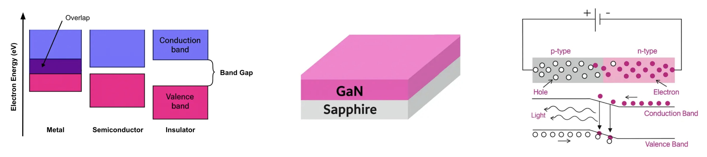
LED technology has been around since the 60s, so why do we not have the life-saving Far-UVC LED yet? The problem is that Far-UVC light requires materials with an ultra-wide band gap which are incredibly hard to find, grow, and dope properly.
However, we’ve faced these hurdles before. In the 90s the blue LED was considered impossible for the same reasons. The history of the blue LED is a story of a select few investors and exceptional scientist who against all odds managed to get the the Blue LED to market. So, how did they do it?
For decades, the world of solid-state lighting was incomplete. Scientists had successfully created red and green LEDs in the 1960s, but a high-efficiency blue LED remained elusive. Without the “B” in “RGB,” creating white light from LEDs was impossible, relegating them to simple indicator lights on electronics. Despite the clear need for the blue LED in society, by the late 1980s, the development of a blue LED was widely considered a dead end by much of the scientific community. Funding dried up and for nearly thirty years no progress was made.
The problem, much like with Far-UVC today, was the material itself. The semiconductor needed for blue light required an exceptionally wide band gap, but this very property is what makes a material so difficult to work with. The tightly bonded electrons that create a wide band gap are also what make it incredibly hard to grow the material into a perfect, defect-free crystal that can then be reliably doped.
The blue breakthrough came from the defiant determination of Shuji Nakamura and some daring investors.
In 1988, while working as an engineer at the small, struggling, Japanese company Nichia Chemicals, Nakamura decided to take on the blue LED. He had read about how Gallium Nitride (GaN) had the perfect band gap for the job, but that even the world’s top labs couldn’t grow it. The founder of Nichia chemicals Ogawa decided to take a significant and unconventional risk by backing Nakamura’s ambitious and unproven research, fronting over $2 million.
With Ogawa’s backing, Nakamura embarked on a one-year placement at the University of Florida to learn how to use the specialised MOCVD (Metal-Organic Chemical Vapour Deposition) reactors that he believed would be the key to perfect GaN crystal growth. Disappointingly, he was isolated from the research group, reportedly being treated as a technician for holding only a master’s degree.
So, with no support from a wider research group, Nakamura began to master a discarded MOCVD crystal growth reactor in a lonely and frustrating process of trial and error. As his attempts got closer and closer to creating the perfect GaN crystal, the ownership of Nichia chemicals changed. Nakamura was ordered to stop all work, with new bosses sticking to the status quo that this was not a commercially viable investment. However, against the explicit instructions of his own managers, Nakamura chose to pursue the synthesis of the “impossible” GaN crystal.
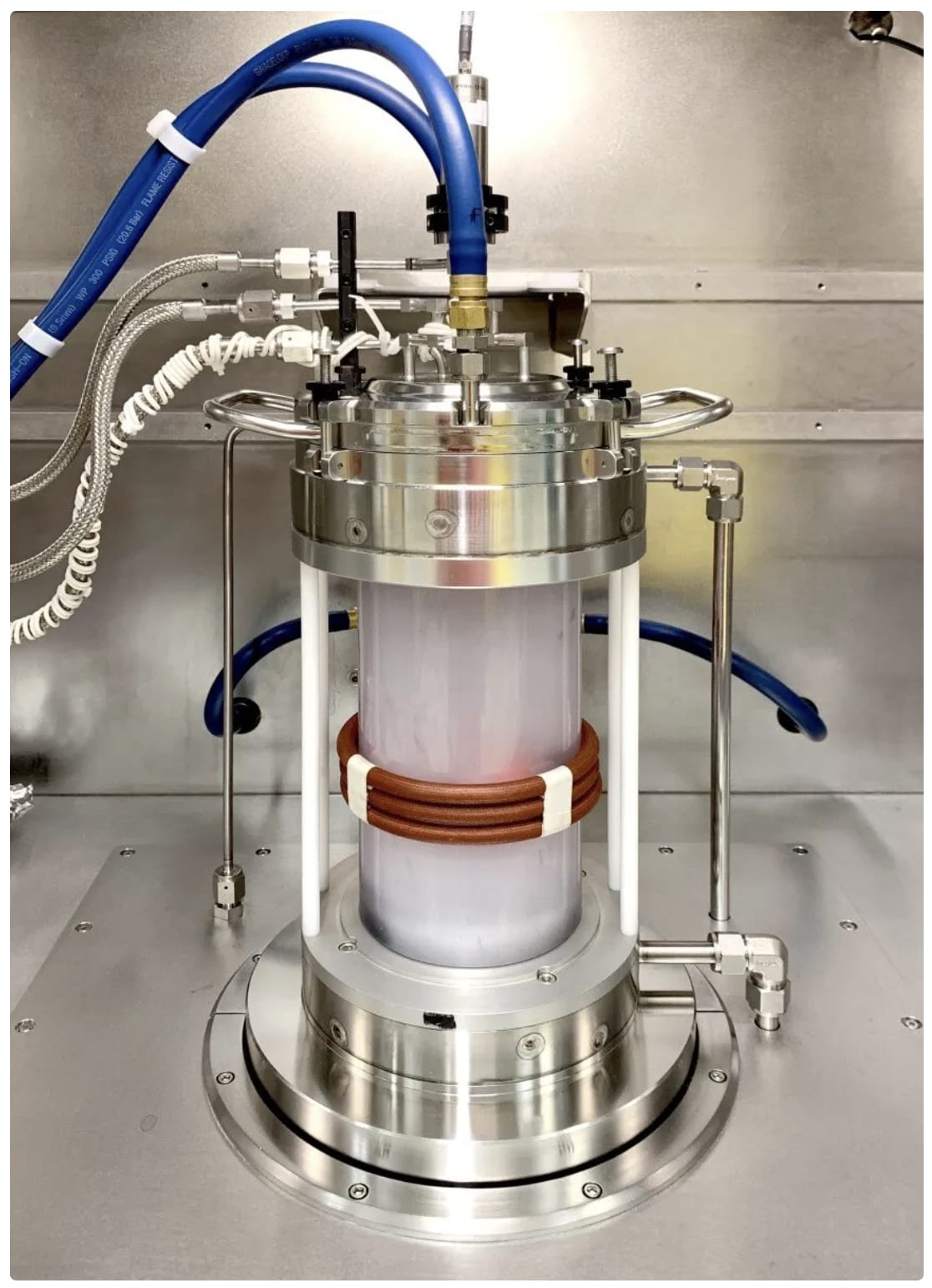
In 1992, after years of painstaking work, Nakamura developed a new “two-flow” method that allowed him to do what no one else could: He grew a beautiful, high-quality GaN crystal, the perfect foundation he had been dreaming of. It was the first great victory in the quest for the blue LED that everyone else had abandoned.
As we know, making the crystal is only half the battle. To form an LED, the perfect crystal then needs to be doped to form a p-type and an n-type. N-type doping was already an understood process involving silicon, however Nakamura still had to create the crucial p-type layer, a problem that had stumped physicists for decades.
Over in another lab, crucial discoveries were being made by Hiroshi Amano and his supervising professor, Isamu Akasaki. They were one of the few researchers in the area to have gained funding for blue LED research. The funding this time came the government, specifically from the Japan Science and Technology Agency (JST) and Ministry of Education, Culture, Sports, Science and Technology (MEXT).
This funding allowed Amano and Akasaki to persist at the impossible doping challenge such that, on one sunny day, they finally found magnesium was the key to successfully p-doping GaN. But, to their crushing disappointment, the crucial “holes” were not active.
In a stoke of luck, while studying the material with an electron beam, they noticed it glowed much brighter where the beam hit it and realised the energy was activating the dopant. Unfortunately this electron beam activation only worked for the surface layer it had hit, and definitely wasn’t a commercially viable manufacturing method for making working blue LEDs.
Back in Nakamura’s lonely lab, filled with discarded firing threats from his bosses, he was determined to develop this p-doping method further. So, without the money for a fancy electron microscope, he decided to try just heating the material up in the oven, a process called annealing. In this simple but revolutionary step, suddenly the p-type layer came to life. This time the heat energy activated the whole p-type semiconductor rather than just the top layer and was also extremely easy to cheaply scale up.
With a working p-n junction, he then rapidly innovated, creating complex quantum well structures that funnelled electrons and holes together with incredible efficiency. So much so the once impossible blue LED now has higher efficiency than its simpler red and green counter parts.
In 1993, Nakamura unveiled a brilliant blue LED, a light so bright and powerful it stunned the scientific community and changed the world forever.
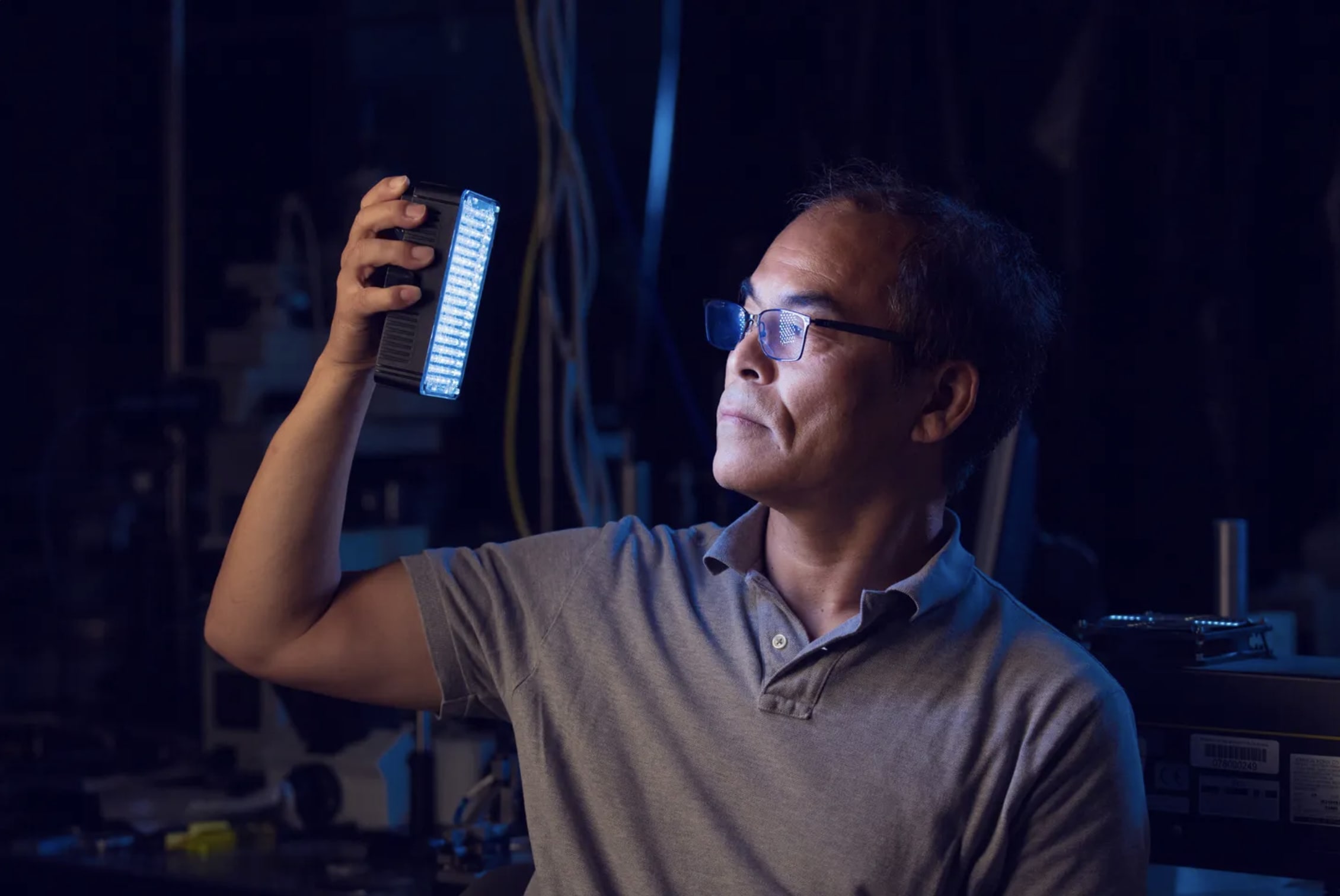
In 2014, Nakamura was awarded a Nobel Prize for his work on Blue LEDs. Since then he has become the Research Director of the Solid State Lighting & Energy Electronics Center, a group that, you guessed it, works on developing UVC LEDs.
So, where does the development of Far-UVC LEDs stand today? The research landscape is rapidly maturing, with efforts focused on high-aluminum-content Aluminum Gallium Nitride (AlGaN). This material is the prime candidate because its band gap can be precisely tuned to the Far-UVC wavelength, while also offering the traditional LED benefits of a small size, long lifetime, and environmental friendliness.
Since 2023, significant progress has been made in AlGaN crystal growth, and researchers can now reliably demonstrate Far-UVC LEDs in a lab setting. The central challenge has now shifted to making them efficient enough to be commercially viable. To achieve this, research is focused on three key priorities: mitigating point defects in the crystal, improving doping efficiency, and increasing light extraction. [4][5][6][7][8]
This work is supported by broad interest in ultra-wide band gap materials for other applications, including advanced sensors and IoT devices. With the shared challenges and increased funding from these adjacent fields I expect innovation will accelerate and that an efficient Far-UVC LED may be on the horizon.
We’ve been focusing on AlGaN materials because they are well known and GaN is now easy to grow, I am curious if theres a new alloy that could provide the required band gap while also being easy to synthesise.
The traditional approach when creating new LEDs has always been “cook-then-look”, a slow, expensive process of trial and error. Scientists would start with a handful of known semiconductors and “cook” them together to create new alloys, hoping to fine-tune the band gap to the exact energy required. Naturally, this process was limited by intuition and the small number of materials they already understood. Now AI can now analyse millions of hypothetical compounds in silico, predicting their band gap and stability before they’re ever made in a lab.
The blue LED was born from years of painstaking and at times heartbreaking research and investment. Its story is a powerful reminder that the invisible innovations of a few dedicated scientists can fundamentally change the world. We now take the technology behind the blue LED for granted, an invention society could not function without.
This is the future I’m hopeful for with Far-UVC: a future where that same dedication leads to a small, cheap, and efficient LED that can be installed everywhere. A future where our air is silently and safely disinfected, making airborne pathogens from the common cold to engineered pandemics a significantly lower threat to humanity.
I’d like to thank Blueprint Biosecurity for providing some of the figures used in this article from their in-depth report on the future of Far-UVC.
Thanks so much for reading! If you found this interesting, please consider sharing it and letting us know what you think.
The Potential Surface is a publication exploring the frontiers of science, technology and AI. It is support by Orbital Materials.
Annabella Wheatley runs the Potential Surface, and is a materials scientist and science writer.
Updated (Oct 7, 2025)


