.png)

In the world of FPGA design, few challenges are as fundamental yet critical as handling external asynchronous signals. Whether it’s a simple push button, a sensor input, or a communication interface, external signals often arrive at unpredictable times relative to our internal clock domains. This unpredictability can lead to metastability—a condition where flip-flops enter an undefined state, potentially causing system failures.
Today, we’ll explore a comprehensive lab that demonstrates proper external signal synchronization techniques. This lab showcases real-world solutions for clock domain crossing (CDC) and debouncing, using a practical button-to-LED interface on the ARTY-Z7-20 development board.
The code for the lab is available on GitHub.
External signals pose several challenges in digital design:
Unknown Timing: External signals have no relationship to internal clock domains
Metastability: When a signal changes near a clock edge, flip-flops can enter undefined states
Mechanical Bounce: Physical switches create multiple transitions before settling
Noise: External signals are susceptible to electromagnetic interference
When a signal changes near a clock edge, the flip-flop may enter a metastable state where the output is neither clearly high nor low. This can propagate through the system, causing unpredictable behavior.
The key to handling asynchronous signals is the multi-stage synchronizer:
module cdc_sync #( parameter integer N = 2, parameter integer WIDTH = 1 ) ( input logic clk, input logic [WIDTH-1:0] din, output logic [WIDTH-1:0] dout ); (* ASYNC_REG = "TRUE", SILISCALE_CDC = "TRUE" *) logic [WIDTH-1:0] sync_reg[N-1:0]; always @(posedge clk) begin for (int i = 0; i < N; i++) begin if (i == 0) begin sync_reg[i] <= din; end else begin sync_reg[i] <= sync_reg[i-1]; end end end assign dout = sync_reg[N-1]; endmoduleThe synchronizer works by registering the input signal on the clock edge. The number of stages determines the MTBF (Mean Time Between Failures) of the synchronizer. The more stages, the higher the MTBF. More than 3 stages is overkill for most applications.
The key aspect here is the ASYNC_REG attribute. This attribute tells the synthesis tool that these registers can handle an asynchronous input on the D input of the flop. For more info, visit the Xilinx UG901.
Key Features:
ASYNC_REG Attribute: Tells synthesis tools these are synchronization registers
Configurable Depth: More stages = higher MTBF (Mean Time Between Failures)
Configurable Width: Handles multi-bit signals
The probability of metastability failure decreases exponentially with each synchronization stage:
MTBF ∝ e^(N × τ)Where:
N = number of synchronization stages
τ = time constant related to flip-flop characteristics
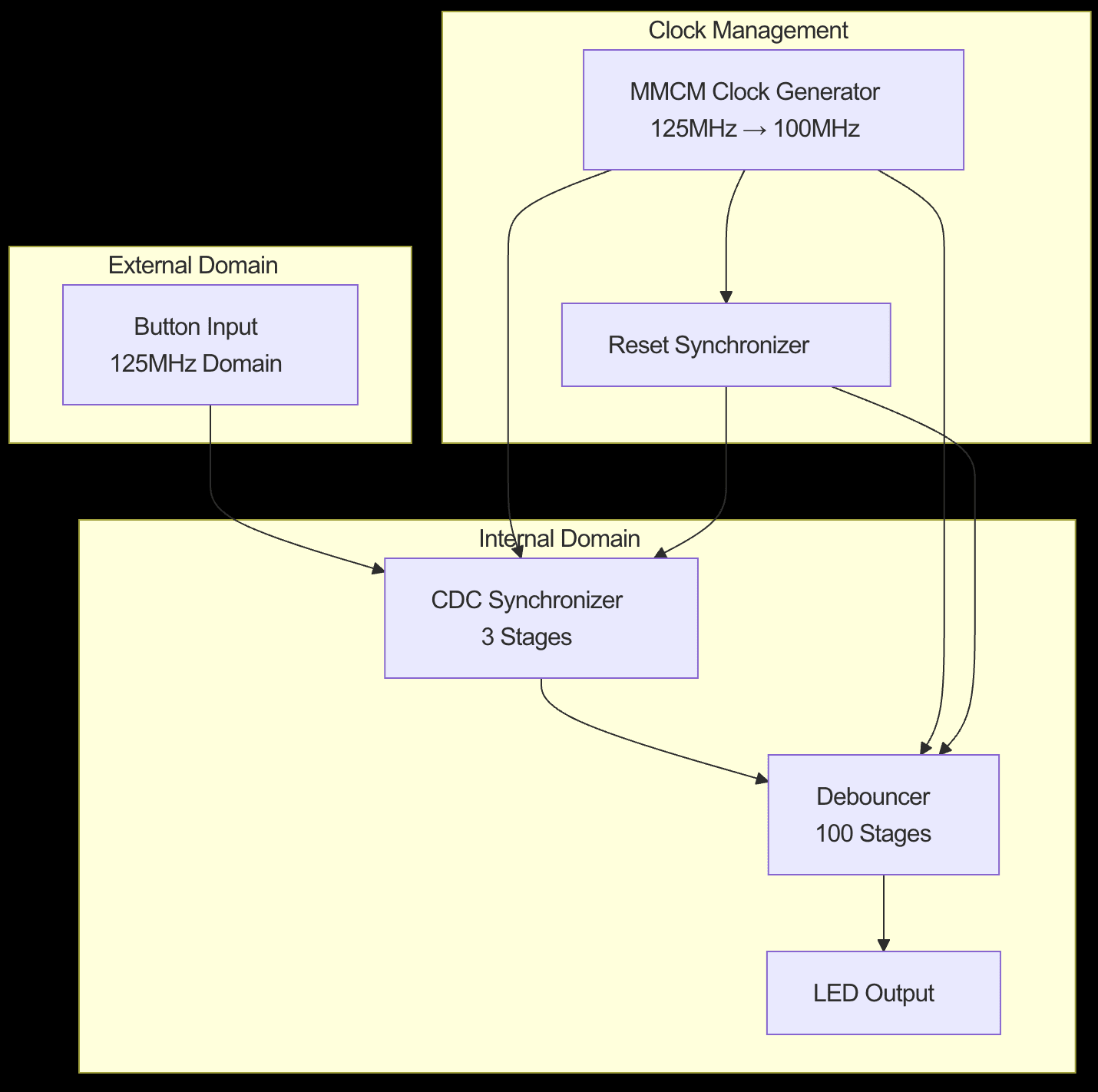
The clock subsystem converts the 125MHz system clock to a 100MHz internal clock:
module clk_rst_subsys ( input logic SYS_CLK, output logic clk_100mhz, output logic rstn_100mhz ); // MMCM configuration for 125MHz → 100MHz conversion MMCME2_BASE #( .BANDWIDTH("OPTIMIZED"), .CLKFBOUT_MULT_F(8), // VCO = 125MHz × 8 = 1GHz .DIVCLK_DIVIDE(1), .CLKIN1_PERIOD(8.0), // 125MHz input .CLKOUT0_DIVIDE_F(10), // 1GHz ÷ 10 = 100MHz // ... other parameters ) MMCME2_BASE_i ( .CLKIN1 (SYS_CLK), .CLKOUT0 (clk_100mhz_mmcm), .LOCKED (locked_mmcm), .CLKFBOUT (clkfbout_mmcm), .CLKFBIN (clkfbout_mmcm) ); // Synchronize the MMCM lock signal cdc_sync #(.N(2), .WIDTH(1)) cdc_sync_locked_i ( .clk (clk_100mhz), .din (locked_mmcm), .dout(rstn_100mhz) ); endmodule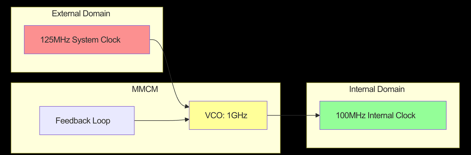

Our implementation uses a 100-stage shift register:
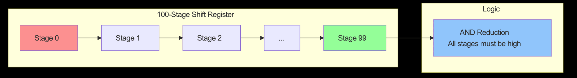
Why 100 Stages?
At 100MHz, each stage represents 10ns
100 stages = 1μs debounce time
Mechanical bounce typically lasts 1-10ms
Conservative approach ensures reliable operation
This AND reduction ensures the LED only illuminates when the button has been stably pressed for the full debounce period.
# Clone the repository git clone <this-repo> cd <this-repo> # Set environment variable export REPO_TOP_DIR=$(pwd) # Initialize SVLib submodule git submodule update --init --recursive # Create Vivado project vivado -mode batch -source tcl/proj.tcl -notrace module fpga_top_tb; logic SYS_CLK = 0; logic BTN0; logic LD0; fpga_top fpga_top_i ( .SYS_CLK(SYS_CLK), .BTN0(BTN0), .LD0(LD0) ); // Generate 125MHz clock (8ns period) always #4 SYS_CLK = ~SYS_CLK; initial begin BTN0 = 1'b0; // Wait for system to stabilize for (int i = 0; i < 100; i++) begin @(posedge SYS_CLK); end // Simulate button press BTN0 = 1'b1; // Run simulation #10000; $finish; end endmoduleThe design must meet several timing constraints:
# Clock constraints create_clock -name SYS_CLK_PIN -period 8.00 -waveform {0 4} [get_ports { SYS_CLK }] # Pin assignments set_property PACKAGE_PIN H16 [get_ports { SYS_CLK }] # 125MHz system clock set_property PACKAGE_PIN D19 [get_ports { BTN0 }] # Button input set_property PACKAGE_PIN R14 [get_ports { LD0 }] # LED outputMulti-stage synchronization: 3 stages for high MTBF
ASYNC_REG attributes: Proper synthesis guidance
Reset synchronization: Clean reset across domains
Shift register approach: Simple, reliable, synthesizable
Conservative timing: 1μs debounce time
AND reduction logic: Ensures stable detection
MMCM usage: Professional clock generation
Feedback loops: Proper VCO configuration
Lock monitoring: Synchronized reset generation
Modular structure: Reusable components
Clear interfaces: Well-defined module boundaries
Comprehensive verification: Testbench coverage
This lab demonstrates techniques used in countless real-world applications:
Safety interlocks: Reliable button and switch handling
Sensor interfaces: Analog-to-digital conversion synchronization
Communication protocols: UART, SPI, I2C interface handling
User interfaces: Button debouncing in remote controls
Touch sensors: Capacitive touch synchronization
Audio interfaces: Sample rate conversion
CAN bus interfaces: Multi-domain communication
Sensor fusion: Multiple sensor synchronization
Safety systems: Critical signal handling
LUTs: ~200 (primarily for debouncing shift register)
Flip-flops: ~105 (100 for debouncing + 5 for synchronization)
MMCM: 1 (clock generation)
Clock domains: 2 (125MHz external, 100MHz internal)
Maximum frequency: 100MHz internal clock
Debounce time: 1μs (configurable via parameter)
CDC reliability: MTBF > 10^9 years with 3-stage synchronizer
Problem: Vivado reports CDC violations Solution: Ensure ASYNC_REG attributes are set on synchronization registers
Problem: Setup/hold timing violations Solution: Check MMCM configuration and clock constraints
Problem: LED flickers or doesn’t respond Solution: Increase DEBOUNCE_FLOPS parameter for longer debounce time
Problem: System doesn’t start properly Solution: Verify MMCM configuration and input clock frequency
For multi-bit signals, consider using:
Gray code encoding: Ensures only one bit changes at a time
Handshake protocols: For complex data transfers
FIFO-based synchronization: For streaming data
Counter-based: More efficient for long debounce times
State machine: More complex but flexible
Analog filtering: RC circuits for simple applications
Vivado CDC Analysis: Built-in CDC checking
Formal verification: Mathematical proof of correctness
Simulation: Extensive testing with various timing scenarios
This lab demonstrates fundamental techniques for handling external asynchronous signals in FPGA designs. The combination of proper CDC synchronization, robust debouncing, and professional clock management creates a reliable foundation for any system that interfaces with the external world.
The key takeaways are:
Always synchronize external signals using multi-stage synchronizers
Debounce mechanical inputs to filter noise and bounce
Use proper clock management with MMCM/PLL components
Follow synthesis guidelines with appropriate attributes
Verify thoroughly with simulation and timing analysis
These techniques form the backbone of reliable digital systems and are essential knowledge for any FPGA designer working with real-world interfaces.
Original post published here https://siliscale.com/ext-sig-sync