.png)

This article concludes a lengthy series. You may be interested in the start of silicon valley, Fairchild, the founding of Intel, the start of the x86 architecture, Intel’s pivot to become a processor company, the i960 and i486, the Intel Inside campaign, the FDIV bug and the Pentium Pro, MMX, the Pentium II, and the Pentium III, Pentium M, Intel Core, and FinFET.
Shockley was a man so repulsive that despite his genius, the people he’d gathered left his company to start Fairchild. Fairchild suffered the fate of many companies becoming so bureaucratic that it paralyzed itself. One of the many Fairchildren was Intel, and Intel was a bit different from the rest because the key people founding it had been leaders at both Shockley and Fairchild. Intel’s first business had been memory. The company then pivoted to microprocessors as the memory business raced to the bottom in pricing. Intel’s greatest strength wasn’t actually logic but fabrication, and while memory and microprocessors were certainly different, the company’s expertise could be applied to either product category. This can be seen in the products the company created. From the earliest days, the 8080 wasn’t the best. The chip’s clone, the Z80, beat it, and the far lower cost 6502 could often beat it. A little later, the 8088 wasn’t the best 16bit CPU. Yet, Intel could deliver in a volume that no one could really match. Then, recognizing the need for better logic, Intel created the P6 where the x86 ISA was translated into RISC-like micro-operations. With the P6, good logic was married to excellent process, and the company managed to overtake even the workstation vendors. Intel briefly fell behind their erstwhile second-sourcer, AMD, but then created the Intel Core 2. This brought the P6 architecture to the 64bit era, and Intel managed to outperform every other microprocessor vendor. The Core 2 chips evolved, became Core i, and Intel was enjoying a near monopoly in the laptop, desktop, workstation, and server markets. The key market they didn’t hold was the extremely power efficient market which was dominated by ARM. Intel had sold its own ARM product line, XScale, some years before. The company attempted to fill that market segment with remade Pentium chips in the form of Intel Atom, and while modestly successful, Atom wasn’t winning.
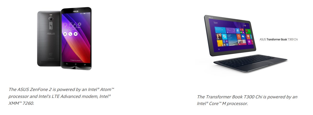
On the 5th of January in 2015, Intel’s Kirk Skaugen took to the stage alongside Jonney Shih of ASUS to introduce the ASUS ZenFone 2 and the Transformer Book T300 Chi. These two devices showcased what Intel could offer to the ultra-efficient world.
On the 6th Krzanich introduced more low-power computing technology in the form of the Intel Curie module intended for wearable devices. Curie was built around the Intel Quark SE SoC which integrated an x86 CPU, sensor hub, bluetooth, 6 axis accelerometor, and charging. It had 384K on-die flash and 80K on-die SRAM and had a TDP of about a third of a watt. So, what was Quark?
The Intel Quark CPU line was first introduced in late 2013 at a price of $9.63 with the X1000. This was a single core i586 part clocked at 400MHz, but it included a single channel DDR3 memory controller, two single-lane PCIe 2 controllers, a USB controller (2x USB2 host, 1x USB2 device), two 10/100 ethernet controllers, SDIO 3, eMMC4, SD3, SPI, UART, and I2C. The X1000 was followed by more SKUs that added things like ECC, Secure Boot, and wider memory addressing throughout 2014. In 2015, following the announcement of Curie, Intel released D1000, D2000, and C1000 series of Quark CPUs which utilized SRAM, had TDPs of 0.025W, and operated at 32MHz. These were i586 class parts that lacked floating point. Prices ranged from $2.54 to $10.32.
On the 2nd of April, Intel announced the 750 series of solid state disks. These were SSDs that used four lanes of PCIe 3 and the NVMe standard. For the consumer market, the company announced the 535 series which were SATA parts ranging from 56GB to 480GB in a 2.5 inch form factor.

On the 5th of August in 2015, Intel introduced the sixth generation of Intel Core, Skylake, built on the company’s 14nm process. For mobile, Skylake chips were available with BGA packaging, and on the desktop parts Skylake used either LGA1151 or LGA2066. All SKUs were intended for Intel 100 series chipsets. From Haswell, Intel had removed the integrated voltage regulator, introduced DMI 3, added support for DDR4, added support Thunderbolt 3, SATA Express, D3D 12.1 for Iris Pro, up to 128MB of L4 cache, HDMI 1.4, DisplayPort 1.2, eDP, and on a few SKUs, HDMI 2.0. On the instruction set side of things Intel added MPX (memory protection extensions) and SGX (software guard extensions), and some Xeon’s gained AVX-512F. This era also brought speed shift, deeper out-of-order buffers, and more execution units. This generation did, however, start breaking backward compatibility. VGA, IDE mode (for SATA), and EHCI were all retired. TDPs for Skylake ranged from 4.5W to 165W, L1 cache was 64K, L2 was 256K per core (though some parts were 1MB), and L3 was up to 38.5MB. The combination of changes differentiated Skylake enough that it would have been the i801186 in Intel’s original naming scheme. Despite all of the changes and modernization that Skylake brought to the table, early benchmarks weren’t exactly amazing. Against Haswell, Skylake offered around 5% to 6% more instructions per clock. On the other hand, for those looking for a new system, Skylake did offer roughly a 37% performance gain compared to Sandy Bridge (second generation Core i).
On the 28th of December in 2015, Intel completed their acquisition of Altera. Altera had been founded in 1983 and focused on the development of field programmable gate arrays, FPGAs. These are integrated circuits that can be reprogrammed after manufacturing using a language like VHDL. Altera had delivered the first FPGA, the EP300, in 1984. Intel’s relationship with Altera began around that time when Altera bought Intel’s programmable logic business for $50 million. In February of 2013, Altera began using Intel’s 14nm process for their chips, and finally, Intel bought the company and Altera became Intel’s Programmable Solutions Group (PSG).
Intel’s CPU offerings were now from low-end to high-end (according to Intel): Quark, Atom, Pentium, Celeron, Core m, Core i, Xeon, Xeon Phi, Itanium. The company was still a maker of cellular modems, Bluetooth and WiFi controllers, GPS receivers, and flash storage devices. Of all of these products, consumer microprocessors (Atom through Core i) represented the majority of Intel’s revenues at 58%. Datacenter microprocessors (Xeon through Itanium) were the next largest share at 29%.
Intel closed 2015 with $55.3 billion in revenue, $11.4 billion in income, $19 billion in cash, $22 billion in debt, $103 billion in assets, and 107,300 employees.
On the 8th of January in 2016, Intel announced Thunderbolt 3 at CES offering speeds of 40Gbps over a USB-C terminated cable.
In April with PSG formed, Intel’s structure was divided into the CCG (client computing group [Atom through Core i]), DCG (datacenter group), IOTG (Internet of things group), NSG (non-volatile memory group), ISecG (Intel security group), and PSG. This restructuring saw Intel dismiss around 12,000 people. Around the same time, Intel canceled their next generation of Atom for phones and tablets effectively ending Intel’s ambitions in those markets. Atom continued for industrial, automotive, and other segments.
New Atom CPUs were released in October with the E3900 series. These little CPUs were targeting TDPs of 6.5W, 9.5W, and 12W and offering either 2 or 4 CPU cores tied to 12 or 18 EUs of Intel’s Gen9 iGPUs. These were also built with Intel’s Time Coordinated Computing Technology offering internal timing synchronization accuracy of 1 microsecond. Intel intended the E3900 for automotive, industrial, and real time video processing market segments. On the video side, the E3900 was capable of 15 simultaneous 1080p inputs at 30fps. Given the automotive market ambitions, the E3900 variant A3900 could operate at temperatures ranging from -40C to 110C. These chips also shipped with an SDK targeted toward Intel’s intended use cases.
Also in October, Intel shipped seventh generation Core i chips, Kaby Lake. These were still on 14nm, but the process was more refined. Kaby Lake largely provided clock speed increases on the CPU side with the L4 cache removed, but the GPU side saw more improvement with HDCP 2.2, HEVC encode and decode, and OpenCL 2.1 support. These were still socket LGA1151 parts.
Intel closed 2016 with $59.3 billion in revenue, $10.3 billion in income, $25.2 billion in debt, and 106,000 employees.
On the 10th of February in 2017, Intel announced that they’d be shipping eighth generation Core i CPUs, Cannon Lake, built on the company’s 10nm process in the second half of the year, and further that they’d be starting work on their 7nm process.
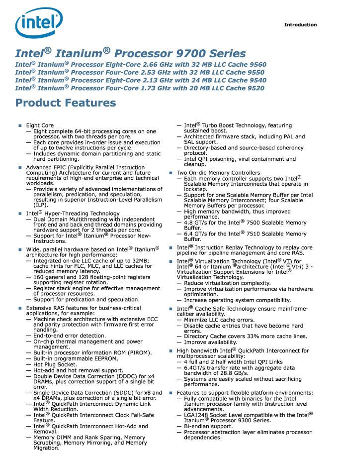
On the 11th of May in 2017, Intel announced that the Itanium 9700 would be the final Itanium. Built on Intel’s 32nm process, the low-end SKU in the series was the 9720 with 4 cores and 8 threads at a base frequency of 1.73GHz built of 3.1 billion transistors. The chip had 20MB of cache, a 6.4GT/s bus, a TDP of 130W, and fit the LGA1248 socket. It supported TurboBoost 2, SpeedStep, VT-i (virtualization), Execute Disable Bit, and extended page tables. The high-end part was the 9760, and it doubled both core and thread counts, bumped the base frequency to 2.66GHz, the TDP to 170W, and the cache to 32MB. All of these CPUs supported DDR3-1067. By this time, the lone remaining customer for Itanium was HPE, and HPE was working toward moving HP-UX customers to x86-64 servers running Linux.
Those 10nm Cannon Lake parts, didn’t arrive. Intel’s 10nm process was delayed, and the company instead released Coffee Lake built on 14nm as the eighth generation series. The primary change here was an uplift in core counts. The Core i3 became a quad core part without hyperthreading, the i5 became a hex core part without hyperthreading, and the i7 became a hex core part with hyperthreading. Coffee Lake also increased L3 cache, pushed clock speeds a bit higher, supported faster DDR4 but removed support for DDR3.
As a result of smartphone proliferation, Samsung surpassed Intel in revenue on chip sales for Q2. Intel reported $14.76 billion while Samsung reported $15.8 billion.
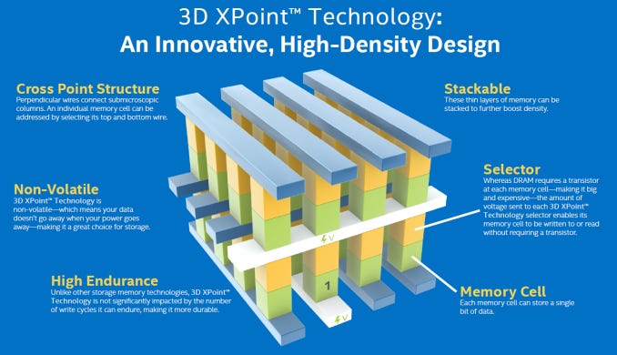
In October, Intel released the Intel Optane 900P NVMe SSD in 280GB and 480GB capacities using four lanes of PCIe 3. The drive had a sequential read speed of 2500MB/s and write of 2000MB/s. The interesting thing about this drive is that it was built with 3D XPoint technology, the basic premise of which is that threshold switches replace transistors. A threshold switch essentially maintains a high resistance until a threshold voltage is reached at which point the switch becomes conductive; it then remains conductive until voltage drops below the holding voltage. The primary advantages in non-volatile memory are size and performance. Memory cells could be made far smaller using threshold switches, and memory reads and writes could be done far more quickly.
Intel closed 2017 with $9.6 billion in income on revenues of $62.7 billion. The company’s assets had grown to $123.2 billion, debt to $26.8 billion, and Intel’s headcount had shrunk to 102,700.
In January of 2018, knowledge of two security vulnerabilities, Spectre and Meltdown, relating to speculative execution were revealed to have affected every Intel CPU supporting out-of-order execution made since 1995. That’s every single Intel CPU except for Itanium and most Atoms. IBM Power CPUs and some ARM CPUs were also affected, and while AMD was largely immune to Meltdown, their chips were susceptible to Spectre. Meltdown exploited a race condition that existed between memory access and privilege checking essentially allowing a process to read memory that wasn’t allocated for it. Spectre operated by exploiting the fact that CPUs engage in speculation before bounds checking, or in Spectre 2, by exploiting the branch target buffer forcing a misprediction and redirecting execution to memory locations where a program wouldn’t naturally go. That Intel was vulnerable to both Spectre and Meltdown was particularly rough as the patches to fix these vulnerabilities impacted performance, and AMD had released their Ryzen CPUs in 2017 on Global Foundries’ 14nm process. Ryzen had already been competitive with Intel’s latest CPUs, and the software mitigations on Intel’s chips allowed first generation Ryzen parts to shine.
On the 19th of April in 2018, AMD’s second generation Ryzen chips were released on GlobalFoundries 12nm process. This again hurt Intel in performance oriented SKUs as the company’s leads on process and logic were threatened. It is worth noting, however, that Intel’s first 14nm process had higher transistor density than GlobalFoundries’ and a lower voltage requirement. The refined 14nm process Intel was using at this point, was further ahead still.

In May, the very first 10nm parts from Intel saw limited release as mobile 9th generation Intel Core i (Cannon Lake), and these were the first mainstream Intel parts to include AVX512 instructions. The chips were socketed for BGA1440, supported DDR4 and LPDDR4, and supported 16 lanes of PCIe Gen3. All of these parts had 64K L1, 256K L2, 2MB per core L3, with a max clock of 3.2GHz, and two physical cores. The integrated GPU was disabled.
On the 21st of June in 2018, Brian Krzanich was removed both from his position as CEO and his position as an Intel board member following the disclosure of his having had a multi-year extramarital affair with a subordinate in violation of the company’s non-fraternization policies. The company’s CFO Bob Swan was then appointed interim CEO.
In July, Bob Swan stated that Intel’s 10nm move had been “too aggressive,” but he also stated that 10nm products should begin volume shipment in 2019.
Intel’s response to Ryzen came on the 8th of October, and it was quite a bit softer than what most Intel fans would have hoped. The ninth generation of Intel Core i was the “Coffee Lake Refresh” on 14nm. These included hardware mitigations for some of the Meltdown and Spectre vulnerabilities, higher clocks, a bump from 6 cores to 8 on the i7, and Turbo Boost on the i3 parts. Surprisingly for a “refresh,” these CPUs did support more RAM, up to 128GB, and the refresh was enough for Intel to keep the title of fastest CPU for most workloads; a statement that wouldn’t have needed to have been uttered as recently as 2016.
Intel’s income for 2018 was $21 billion on revenues of $70.8 billion. The company’s debt was $25 billion, assets were $127.9 billion, and the company employed 107,400 people.
Intel did indeed finally launch 10nm products in 2019, and it was an improved 10nm process over that used for the limited release Canon Lake parts. These parts, however, were only mobile or Xeon, and no desktop parts were released. In September of 2019, Ice Lake hit the market and was considered 10th generation. These parts could clock up to 4.1GHz, had 80K L1 (32K instruction, 48K data), 512K L2 per core, and up to 8MB of L3. They had 2 or 4 cores, and featured Intel Xe graphics. As far as new features went, the highlights were Dynamic Tuning 2 allowing the CPU to sustain turbo frequencies for longer periods of time, a better branch predictor with a global history size of 194 branches, hardware accelerated SHA, Deep Learning Boost for the acceleration of AI workloads, and PCIe 4 support. On the GPU front, these parts had up to 64 execution units, could support 4K at 120Hz (or 5K or 8K at lower refresh rates), variable rate shading, DisplayPort 1.4a, HEVC and VP9 encode/decode, and better image scaling.
More interesting than the CPUs themselves was Intel’s 10nm process. Intel 10nm had a transistor density (around 100 million per square millimeter) that was roughly 2.7x the density achieved on Intel 14nm, and it was around 1.7x denser than any other 10nm node. This process node also offered around a 60% reduction in power consumption and 25% performance uplift compared to Intel’s first 14nm process. The company achieved a fin pitch of 34nm, a fin width of 7nm, and a fin height of 53nm. The contacted gate pitch was around 54nm, the minimum metal pitch was around 36nm, and the gate length was around 20nm. Getting to this wasn’t easy, and it involved yet another breakthrough. Shrinking to this scale meant that interconnect barrier layers were taking up most of the interconnect area, and shrinking copper increases resistance. The company then chose to swap copper for cobalt which allowed them to shrink the barrier layer. This worked because cobalt has a larger grain size. In large volumes, cobalt has a higher resistance than does copper, but at the geometries Intel was dealing with, it had a far lower resistance, lower electron scattering, and a far higher resistance to electron migration.
Intel’s 10nm node also introduced Foveros. Foveros is a packaging technology in which two or more chiplets can be assembled together with a base logic die having components stacked on top of it using 36 micron little bumps of metal. This allows things like memory or an FPGA to be placed in the same package as a CPU.
While Samsung and TSMC had done better than Intel’s 14nm process, their 10nm nodes were closer to Intel’s 14nm than they were to Intel’s 10nm. And, judging by transistor density, TSMC’s 7nm process was roughly equivalent to Intel’s 10nm process achieving around 91.2 million transistors per square millimeter. Samsung’s 7nm process achieved around 95.08 million. Intel made quite the achievement despite being quite late. Yet, this achievement wasn’t as great as it might have been. Intel’s competition had made dramatic leaps and were now able to compete with them on fabrication. Had Intel kept their original pace, this would have been impossible. The fact that the marketing of 10nm vs 7nm wasn’t well understood and most people viewed the smaller number as being superior also hurt. Then, in actual shipping products, AMD’s Zen 2 utilizing chiplets on TSMC’s 7nm was good with Epyc Rome and the 3000 series of desktop parts being competitive in both price and performance against Intel’s product portfolio.
By the end of 2019, Intel had a presence in Oregon, Arizona, New Mexico, Ireland, Israel, Chengdu, Malaysia, Vietnam, and Dalian. CCG accounted for 52% of the company’s revenues, DCG 33%, NSG 6%, IOTG 5%, and PSG 3%. Intel closed 2019 with $21 billion in income on $71.9 billion in revenue.
I don’t imagine that 2020 was a good year for anyone, and Intel was no exception. The company announced a delay in their 7nm rollout, Jim Keller who’d joined the company in 2018 to help get them to the finish line on 10nm departed the company, and Apple announced that they’d be moving all of their systems to their own ARM-based CPU designs. Apple’s move, according to themselves, was due to Intel’s inability to supply them with sufficient quantities of hardware, and then for the hardware they did get it had poor performance per watt, and bad thermals. I think there was also likely an ecosystem play in mind for the company, but I am sure Intel’s struggles didn’t hurt their decision.
Intel launched the 11th Generation of Core i CPUs, Tiger Lake, on the 2nd of September in 2020, and these were again mobile-only parts. They supported DDR4 and 20 lanes of PCIe 4.
On the 20th of October, Intel announced that they’d reached a deal to sell their NAND flash business to SK Hynix for around $9 billion. At this time, Intel accounted for roughly 11% of the NAND market and SK Hynix accounted for roughly 12%. Even after the merger, SK Hynix would be the second largest in the market after Samsung who represented 31%. For SK Hynix this deal would give them a larger share of the market, and for Intel the deal would allow them to be rid of a business unit that had just lost $340 million over the prior 12 months. This deal would play out in two phases. First, SKH would take over the physical assets, and second the company would take over the intellectual property and staff.
Intel ended the year with $20.89 billion in income on revenues of $77.8 billion.
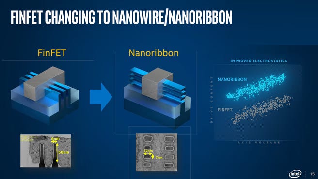
Pat Gelsinger returned to Intel as CEO on the 15th of February in 2021. One month later, Gelsinger announced a new corporate strategy called “IDM 2.0” that focused on a rejuvenation of Intel’s core engineering expertise. This strategy included Intel’s vertically integrated x86-64 and peripheral chip design and manufacturing, the use of external foundries, and the introduction of Intel Foundry Services to manufacture chips for other companies. Taking back the lead in fabrication technology would include five nodes in five years: 7nm, 4nm, 3nm, 20A, 18A. Though, Intel chose to rename these nodes dropping the nanometer designation while keeping the angstrom designation, so these were then Intel 7, Intel 4, Intel 3, Intel 20A, and Intel 18A. With these, Intel would continue to use DUV lithography for 7, would use EUV for 4, 3, and 20A, and then transition to High-NA EUV for 18A. Starting with 20A, Intel would transition to RibbonFET from FinFET. RibbonFET is a form of Gate-All-Around transistor which wraps the gate around the channel allowing for extremely precise control of current flow.
On the 30th of March in 2021, Intel launched Rocket Lake on their 14nm process supporting up to 128GB of DDR4, and Intel Thermal Velocity Boost on Core i9 parts. These were the 11th generation desktop parts in Intel’s line up.
On the 4th of November in 2021, Intel released their Alder Lake CPUs fabricated on Intel’s 7nm process. These supported up to 128GB of either DDR4 or DDR5, had up to 32EUs of integrated graphics on desktop or 96 on mobile, and featured heterogenous cores with Performance (P) and Efficiency (E) cores in the same CPU. The P cores featured dedicated floating point adders, six instruction decoders, larger re-order buffers, and larger micro-op cache. Overall, the CPU has a few new instructions, 1 TB/s interconnect between cores, a new thread director to aid the OS thread scheduler with thread assignment to P and E cores, and 4MB to 30MB of L3. These parts used LGA1700 on desktop and BGA1744 on mobile, and offered 16 PCIe 5 lanes and 4 PCIe 4 lanes. Intel’s 12th Generation Core i was different enough from those preceding it that it would have been considered the i801286 in Intel’s original naming scheme.
Intel ended 2021 with $19.8 billion in income on revenues of $79 billion, and the company’s workforce had grown to over 121,000. The company’s long term debts had grown to $33.5 billion, and assets had grown to $168.4 billion. The first phase of the sale of Intel’s NAND business contributed $6.61 billion, and transferred Intel’s NAND fab in Dalian to SK Hynix. What had once been Intel’s NAND business was now Solidigm.
In January of 2022, Intel selected the greater Columbus area for a new fab. This was set to be a $20 billion investment with the site spanning 3190 acres. The investment would grow over the course of a decade to total of roughly $100 billion. Another site was chosen in Magdeburg, Germany and announced around the same time. Construction at both sites was set to begin in 2023, carry through 2024, and then start producing in 2025 to 2026.

On the 30th of March, Intel announced their re-entry into the discrete GPU market with the Intel Arc brand. The first generation was Alchemist which spanned the models (from low-end to high): A310, A380, A580, A750, A770 8GB, and A770 16GB. The A310 was made of 7.2 billion transistors on TSMC’s 6nm process, contained 6 Xe cores, 4MB of L2, had a clock of 2GHz, and packed 4GB of GDDR6. The A770 was built of 21.7 billion transistors with 32 Xe cores, 16MB of L2, was clocked at 2.1GHz with a 2.4GHz boost clock, and had either 8GB or 16GB of GDDR6. The first card released was the A380 in June. The A310 launched in September while the A580, A750, and A770 released in October. The cards were praised for diversifying the market, offering great price points, and generally providing competition to AMD and NVIDIA, but they did draw quite a bit of criticism for poor driver support at launch. Over time, Intel improved this situation, and the lineup became a decent option for the low-end and mid-market.
On the 22nd of October in 2022, Intel launched the 13th Generation of Intel Core i, Raptor Lake, fabricated on Intel 7. These processors brought boost clocks of up to 6GHz, support for up to 192GB of DDR5 RAM, and these were still made for the LGA1700 socket.
Intel’s revenues for 2022 accounted to $63 billion and income fell to $8 billion.
On the 31st of January in 2023, Intel announced cost cutting measures including reductions to compensation for all midlevel and higher employees, suspension of pay raises, suspension of profit sharing bonuses, and reductions to 401(k) matching.
On the 17th of October in 2023, Intel released their 14th Generation Core i CPUs, Raptor Lake Refresh. These were not different from the preceding generation in any major way. The company largely changed some of the core counts and core assortments, mixing up P/E cores in different numbers.
In December of 2023, Intel launched their Meteor Lake CPUs as the Intel Core Series 1 and Intel Core Ultra Series 1 CPUs. The Intel Core series was comprised of Core 3, Core 5, and Core 7 while the Core Ultra series was comprised of Core Ultra 5, Core Ultra 7, and Core Ultra 9. These chips were manufactured as multichip modules connected with Intel’s Foveros packaging. The compute tile was fabricated on Intel’s 4nm process, the graphics tile was fabricated on TSMC’s 5nm process, and the SoC and the I/O extender were fabricated on TSMC’s 6nm process. Those tiles were then placed on the Foveros interposer base which was fabricated on Intel’s 16nm process. The TDP’s for these chips ranged from 5W to 125W with P cores having a max clock of 5.1GHz, E cores a max of 3.8GHz, and Low Power E cores a max of 2.5GHz. Caches were different between core types with P cores have 112K total L1 (64K instruction, 48K data) and E/LPE cores having 96K L1 (64K instruction, 32K data). P cores had 2MB of L2 per core, while E and LPE cores had 2MB per cluster. The largest L3 cache was 24MB. Given this rather serious change in manufacturing and packaging and the addition of VNNI instructions, Meteor Lake CPUs would have been the i801386 series in Intel’s original naming scheme. Meteor Lake’s reception was tepid at best as the P cores suffered from lower instructions per clock than the previous generation.
Intel’s revenues for 2023 were down to $54.2 billion and income fell to $1.6 billion. The company’s debt burden was up to $49.2 billion. While Intel’s fortunes have historically fluctuated this was a sharp drop year to year in a general downward trend. As far as I can tell, this was due to three factors. The first was a drop in desktop and laptop sales with a concomitant drop in margins. In 2021, CCG brough in $41.1 billion, this fell to $31.8 billion in 2022, and then to $29.3 billion in 2023. The second was the company’s spend on property, plants, and equipment increasing by $16 billion from 2022 levels to a total of $96.6 billion. The company’s datacenter and AI revenues had been also been falling with revenues there in 2021 having been $22.8 billion. This fell to $19.4 billion in 2022, and further to $15.5 billion in in 2023. In short, Intel wasn’t selling as much and the company was spending quite a sum on fabrication improvements.
In early February of 2024, reports surfaced on Reddit and YouTube regarding instability in Intel’s 13th generation and 14th generation CPUs. By late February, the problem was becoming more widely known and experienced with random crashes, out-of-video memory errors, and in some cases catastrophic chip failures. By late April, some motherboard vendors were making UEFI updates available to end-users which sometimes helped and sometimes didn’t. By early July, return rates for 13th and 14th generation processors were 300% to 400% higher than 12th generation chips. On the 25th of September in 2024, Intel identified the root cause as “reliability aging” under elevated voltage and/or temperature of a clock tree circuit. This resulted in four multiple mitigation strategies relating to power and thermal settings and microcode.
On the 29th of February in 2024, Intel announced that they were going to reinstate Altera as an independent and wholly owned subsidiary.
On the 1st of August, Intel announced a 15% workforce reduction and their intent to cut expenses by roughly $10 billion over the rest of the year following the release of Q2 earnings which showed a $1.6 billion loss. Pat Gelsinger wrote:
Simply put, we must align our cost structure with our new operating model and fundamentally change the way we operate. Our revenues have not grown as expected – and we’ve yet to fully benefit from powerful trends, like AI. Our costs are too high, our margins are too low. We need bolder actions to address both – particularly given our financial results and outlook for the second half of 2024, which is tougher than previously expected.
These decisions have challenged me to my core, and this is the hardest thing I’ve done in my career. My pledge to you is that we will prioritize a culture of honesty, transparency and respect in the weeks and months to come.
The second generation of Intel’s new Core series, Arrow Lake, was announced on the 10th of October. This brought the Foveros design to the desktop with the LGA1851 socket. Performance for these parts was intended to be roughly comparable to Raptor Lake parts, but with far better energy efficiency. Like Meteor Lake, Arrow Lake did suffer lower performance than prior generations in some areas, and the company attempted to address this with microcode updates. Unfortunately, these updates didn’t completely ameliorate the situation.
On the 1st of November in 2024, Intel was removed from the Dow Jones Industrial average after 25 years following a share price plunge of 54% over the course of the year.
On the 1st of December in 2024, Pat Gelsinger left both the company and the company’s board. This was reported as a resignation, but it was something more similar to being fired. The board of directors apparently felt that Gelsinger’s expensive turnaround plan had worked neither well enough nor fast enough, and they then gave him the option of resigning or being fired. He chose to resign. In his place were two interim co-CEOs: David Zinsner (CFO), and Michelle Johnston Holthaus (GM of CCG).
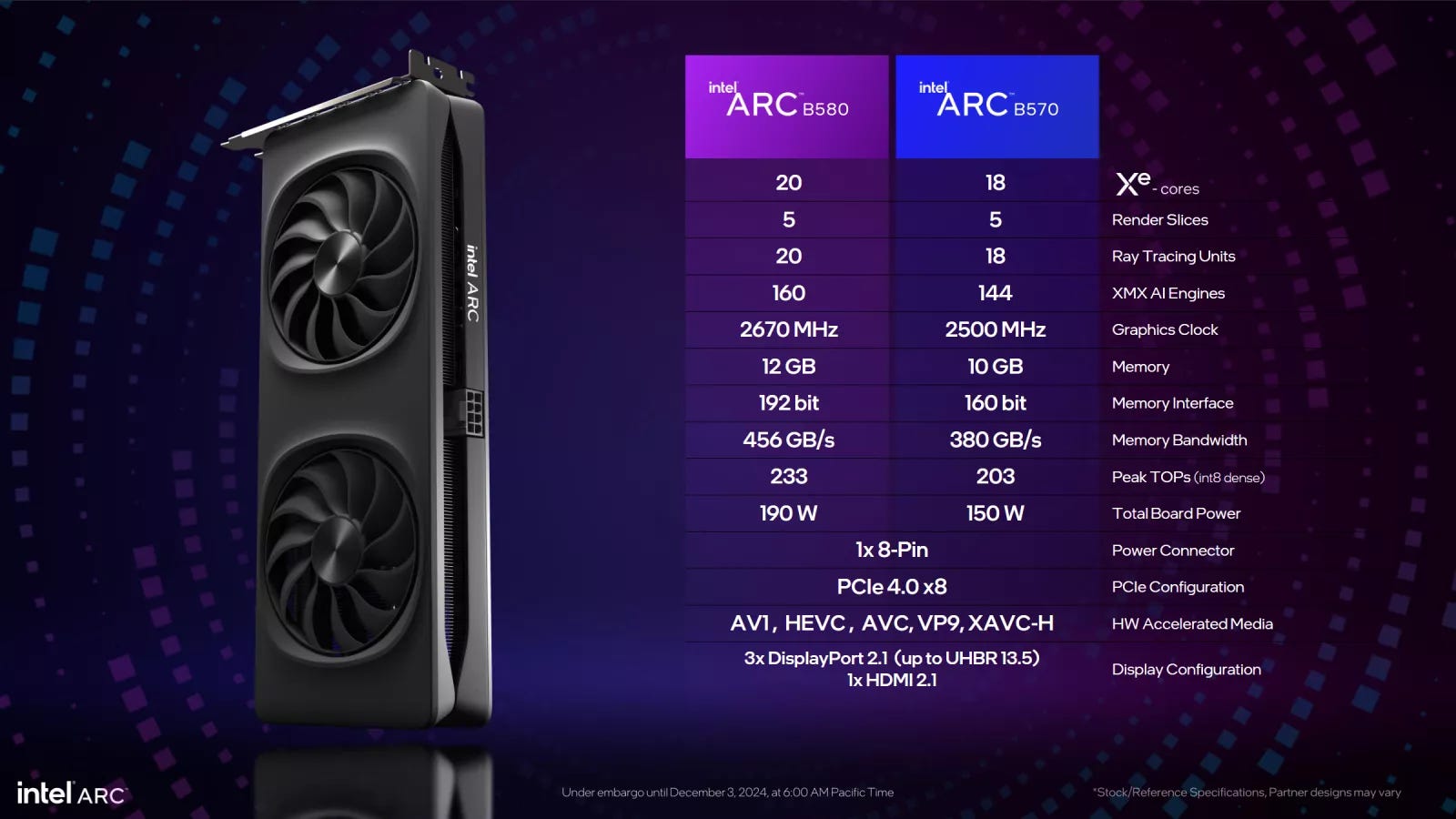
On the 3rd of December, Intel announced two Intel Arc Battlemage cards, the B570 and B580. These cards have 10 and 20 Xe cores respectively with base clocks of 1.7GHz and boost clocks of 2.5GHz and 2.67GHz respectively. The B570 has an L1 cache of 2.5MB and an L2 of 10MB with 10GB of GDDR6 while the B580 has 5MB of L1, 12MB of L2, and 12GB of GDDR6.
Intel closed 2024 with a loss of $19.233 billion on revenues of $53.101 billion. The company had 108,900 employees and $196.5 billion in assets.

Lip-Bu Tan was born on the 12th of November in 1959 in Muar, Johor, Malaysia. He graduated from Nanyang University in Singapore with a Bachelor of Science in physics. He then moved to the USA and earned his Masters from MIT in nuclear engineering. Tan started the journey toward earning his PhD, but left MIT for the University of San Francisco where he earned an MBA. With three older sisters and an older brother who were all extremely accomplished, Tan felt he was the loser of his family. After school, Tan went to work first for EDS Nuclear, then on to ECHO Energy Consulting. When ECHO was sold, Tan went to work for Chappell & Company (investment banking firm). This lasted until Tan was hired by the Walden Group (VC firm) to expand the company into Asia. Tan quickly rose within the company to become a senior partner. In 1987, Tan and Peter Liu founded Walden International as an Asian branch of the company. In 2009, Tan took a CEO position at Cadence Design Systems, but he held onto his chairmanship of Walden. Tan was active with Cadence until 2023, and he was hired by Intel as CEO on the 12th of March in 2025.
Later in March, Intel and SK Hynix finalized the sale of Intel’s NAND business with Intel’s IP, R&D resources, and staff transferring to Solidigm. For this, Intel received $1.9 billion.
On the 14th of April in 2025, Intel confirmed that they still intend to build in Magdeburg, but construction at the site would not begin until 2026 at the earliest. On the 28th, Intel announced that their fab in central Ohio would not be completed until 2030. On that same day, Intel announced that they’d be selling 51% of Altera to Silver Lake.
On the 24th of April in 2025, Lip-Bu Tan announced that the company would be undergoing another round of layoffs (some rumors have stated up to 20% of the workforce), a restructuring, $1.5 billion in cost reductions, and the expansion of an in-office mandate. Calling his intentions a restructuring may be an understatement as he said he intends to cease the “bureaucracy suffocating the innovation and agility that we need to win.” And, I mean… he’s not wrong as some teams have up to eight layers of management. This announcement followed Q1 earnings which showed CCG down 8%, DCAI up 8%, Foundry up 7%, overall revenue flat compared to Q1 2024, and the company posted a loss of $800 million (roughly double the loss of Q1 2024).

Intel’s downward trajectory started in 2015 with the delay of 10nm which provided TSMC, Samsung, and GlobalFoundries the time needed to make progress. This delay was most likely due to high amounts multi-patterning as a result of sticking with DUV as opposed to EUV. While all manufacturers use multi-patterning, high amounts of multi-patterning increases the chance of a defect meaning yields drop until the company can rid the process of errors, and in some cases Intel was using six exposures to create single features. The lower the yield the higher the cost per wafer which can make the entire process node uneconomical. There’s also an increase in time required for each wafer every time another exposure is added to the process. When Intel says that it was “too ambitious,” the chart of transistor density there is showing what was meant. The company’s jump in density was far more similar to that of their competitors’ 7nm, and as Intel refined the 10nm process it improved further still. Intel’s lead in the market had always been their expertise in fabrication, and that was no longer winning for them. So, in short, Intel’s choice to stick with DUV for an incredibly advanced process was the primary cause of Intel’s current position.
Finally, this was a long series. Even at this length, there is more that could be said about all that Intel achieved over the years. I’ve left out quite a bit. As Intel has long been the CPU company and CCG provided the majority of the company’s income, that was my focus. Most regrettably to me, however, is that when companies grow to immense sizes with complex bureaucracies, individuals’ contributions are harder to track. To every single present and former Intel employee, thank you for your contributions to our industry.
I have readers from many of the companies whose history I cover, and many of you were present for time periods I cover. A few of you are mentioned by name in my articles. All corrections to the record are welcome; feel free to leave a comment.