.png)

Introduction
The surging need for precision medicine presents a significant challenge for nuclear medical imaging technologies, particularly single-photon emission computed tomography (SPECT), requesting a boost in energy resolution (ER), detection sensitivity, and spatial resolution. In SPECT, a single-photon γ-ray “camera” detects trace amounts of substances labeled with γ-ray emitting radionuclide (e.g., 99mTc, 131I, 177Lu)1,2. Unlike imaging modalities such as computed tomography and magnetic resonance imaging, which primarily visualize anatomy, nuclear medicine imaging provides the spatially resolved physiological information relating to metabolic processes by localizing emitted γ-rays, offering diagnostic insights of a wide range of tumor states3,4. Currently, SPECT is commonly accessible and routinely used for clinical diagnosis and radionuclide therapy, with prominent prognostic value5,6.
The key component of SPECT is the single-photon γ-ray camera, which spatializes the specific γ-rays. γ-ray cameras in SPECT utilize two main detection mechanisms, indirect photoconversion by scintillators coupled with photomultiplier tubes and direct photoconversion by semiconductors7,8. For a conventional scintillator γ-ray camera, a 9.5 mm-thick NaI(Tl) crystal is needed to attenuate approximately 92% of the 141 keV γ-ray photons with an ER of 9.8% (Supplementary Fig. 1 and Supplementary Table 1). The intrinsic spatial resolution is around 5 mm, and the sensitivity is about 1 to 2 × 10⁻⁴ cps/Bq1,9. In semiconductors, the charge carriers exhibit less spatial dispersion, and pixelated signal readout enables superior spatial resolution10,11,12,13. Thereby, a γ-ray camera equipped with pixelated CdZnTe (CZT) detectors has demonstrated an improved ER of 5.5% at 141 keV and enhanced image clarity with intrinsic spatial resolution of 2.8 mm, which dramatically reduces patient radiation exposure and shortens the examination time12,14 (Supplementary Table 2). Nevertheless, despite the unmatched advantages, the market penetration of semiconductor detectors is still lagging that of conventional scintillators owing to their high cost, which results from persistent unsolved issues in crystal growth. The poor charge transport of holes in CZT, resulting in excessive carrier trapping and a low energy tail, may lead to a deficit in sensitivity15.
Perovskite semiconductors feature characteristics of promising spectral performance and incomparable superiority over cost, positioning them as strong contenders for nuclear medicine imaging15,16,17,18,19,20,21,22,23,24,25,26,27. Since the first report in 201328, considerable efforts have been devoted and yielded enhanced γ-ray detection capabilities29. CsPbBr3 is one of the most attractive candidates because it can readily scale up by melt growth, but with low cost. In our previous work, hole-only sensing CsPbBr3 detectors (quasi-hemisphere and pixelated) exhibit an ER of 1.4% for 662 keV30. Solution-grown crystal also exhibited impressive ER of 1.7%31. As such, perovskite semiconductors arise as a promising alternative for nuclear medicine imaging, and their superior stopping power over CZT may deliver imaging panels with higher sensitivity. However, their utilization in SPECT, particularly single-photon γ-ray imaging, remains uncharted territory.
In essence, the ER of the γ-ray detector is a metric that dominates the radionuclide identification and scatter rejection in γ-ray imaging. Therefore, a better ER is rather desirable to avoid spectral blurring and assure the fidelity of the reconstructed images1. In principle, the theoretical ER of a certain semiconductor is determined by the statistical variance of photon-generated charge carriers measured by the Fano factor32,33. In CsPbBr3, ER driven only by the Fano factor is accordingly predicted to be 0.210% at 662 keV15,29,30, which is far beyond the experimental ER achieved so far. Meanwhile, the non-uniformity caused by charge transport variance is regarded as the essential factor that determines the practical ER in semiconductor detectors34. The charge collection process involves both carrier transport through the crystal bulk and across the perovskite/electrode interface. Despite the reported remarkable charge carrier transport properties in CsPbBr3, charge losses at the interface, which are attributed to imperfections such as defects or mismatches, are often overlooked and still present in prohibiting perovskite semiconductor detectors from attaining near-unity charge collection efficiency (CCE) with high uniformity31,35. Therefore, unveiling the carrier transport variance quantitatively is requested for further improving the ER and achieving single-photon γ-ray imaging.
In this work, we present a proof-of-concept perovskite γ-ray camera designed to image single γ-ray photons for nuclear medicine imaging, offering unparalleled spectral and spatial resolutions. The uniformity of CCE on the surface was quantified through the in-situ photoelectrical response micromapping (PEµM), and further improved to close to unity by chemical-mechanical surface processing, resulting in exceptional uniformity and long-term device stability. A multiple-channel electronics readout system of up to 17 channels was developed for γ-ray imaging. CsPbBr3 detectors were configured to 4 × 4 pixels, and weighting potential optimization and depth analysis enabled record overall ERs of 2.8% at 122 keV, 2.5% at 99mTc 141 keV, which is superior to the current CZT system (Supplementary Table 2), and 1.0% at 137Cs 662 keV. The best ERs from a single pixel were 2.4% at 122 keV, 2.2% at 141 keV, and 0.87% at 662 keV. Single-photon γ-ray imaging by pixelated CsPbBr3 detectors revealed remarkable detection sensitivity for the short half-life 99mTc radionuclide, reaching 0.13%–0.21% cps/Bq through single parallel hole and line collimators. Moreover, Derenzo phantom imaging indicated the spatial resolution is about 3.2–3.8 mm.
Results
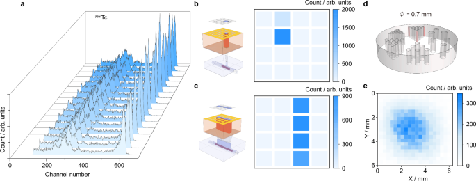
As schemed in Fig. 1a, a perovskite γ-ray camera is proposed and developed for radionuclide γ-ray imaging, consisting of a tungsten collimator, a perovskite CsPbBr3 pixelated detector, and a multichannel signal readout system. Specifically, the γ-ray photons, emitted from the decay of 99mTc in a Na99mTcO4 solution, are captured and converted into electrical signals by the pixelated detectors after passing through the collimator. 99mTc, as an isotope of technetium, possesses γ-ray decay with a single energy of 141 keV and a half-life period of 6.02 h, which is one of the most commonly used radionuclides in SPECT. By quantifying the photon events within a specific energy deposition window for each pixel, the spatial information of radionuclides can be obtained from the projection images of γ-ray photons.
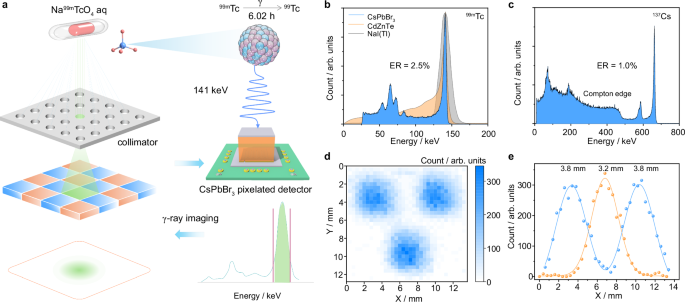
a Schematic illustration of 99mTc γ-ray imaging by perovskite γ-ray camera using 4 × 4 pixelated CsPbBr3 detectors. b Comparison between pixelated CsPbBr3 detector (Device E in a dimension of ~7.0 × 7.0 × 3.6 mm3 under 400 V), CZT (16 × 16 pixelated Imarad CZT module with the pixel size of 2.46 × 2.46 mm2 and detector thickness of 5.0 mm)52 and NaI(Tl)52 under 99mTc γ-ray source. c Overall 137Cs γ-ray spectrum collected by Device I (~8.0 × 8.0 × 5.6 mm3) after depth correction and removing near-pixel events within 25% of the thickness close to the cathode. d 99mTc γ-ray single-photon image of the three-column sources with a diameter of 0.7 mm in the micro Derenzo phantom. e Count profile of the γ-ray image.
Pixelated CsPbBr3 semiconductor detectors with different pitch sizes and detector thicknesses are optimized and fabricated (Supplementary Fig. 2), and have achieved the overall ER of 2.5% for 99mTc 141 keV γ-ray (Fig. 1b) by merging all pixel events. The spectroscopic peak with high photo-fraction and nearly devoid of low-energy tailing highlights its substantial strengths in imaging fidelity. Furthermore, the overall ER for 137Cs 662 keV γ-rays at 1.0% is also demonstrated, alongside a high peak-to-Compton (P/C) ratio of ~6.3 (Fig. 1c). This outperforms the resolution of 1.4% achieved by the thinner planar detector (thickness of 1.33 mm)30. For phantom imaging, Na99mTcO4 aqueous solution sources were positioned in a Derenzo phantom at an imaging distance of 2.05 cm. Leveraging the exceptional spectral resolution, we demonstrate a clear differentiation of individual 99mTc γ-ray sources (Fig. 1d), yielding a system spatial resolution of 3.2–3.8 mm (Fig. 1e).
Spectroscopic grade CsPbBr3 crystals are prepared by the improved Bridgman melt method30 with a ingot diameter of 30 mm. Optical transmittance of the as-grown single crystals is impressively high, nearly 80%, revealing the absence of significant optical absorption centers, as shown in Fig. 2a. The steady-state photoluminescence (PL) centered at 543 nm corresponds to the bound exciton emission. In particular, the PL lifetimes, which are related to the recombination behavior of photogenerated carriers, can be significantly influenced by the presence of defects. The long PL decay time with a rapid component of 76 ns and a slower component up to 276 ns (Fig. 2b), which are comparable to those of previous reported spectral-grade CsPbBr3 single crystals17,29,30,36 confirms a few non-radiative recombination centers and high crystalline quality. The lower trap densities (~2.1 × 1014 cm−3) of the shallow traps compared to prior CsPbBr3 crystals (~1015 cm−3)29 well support the detector-grade quality29,37, validated by thermally stimulated current spectroscopy (Supplementary Fig. 3, Table 3 and Note 1). The hole mobility was estimated as 31 ± 0.26 cm2/(V·s) through the 241Am α particles transient pulse measurement (Supplementary Fig. 4). Notably, the CsPbBr3 detector showcases a strikingly long lifetime of holes up to hundreds of microseconds, making thicker detectors with high efficiency feasible.
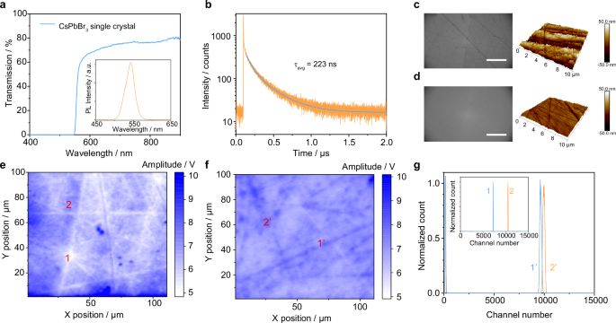
a Transmission spectrum of CsPbBr3 single crystal; inset: photoluminescence spectrum excited at 405 nm. b PL lifetime emission at 543 nm. Roughness comparison of the surface processed by only mechanical polishing (c) and a combination of mechanical polishing and DMSO etching (d); the bar is 0.2 mm. Pulse height mapping of crystal surface processed by only mechanical polishing (e) and chemical-mechanical polishing (f) stimulated by pulsed laser at 482 nm with a duration of 75 ps and a 2 kHz repetition rate. g The energy spectra of a 482 nm ps laser collected from different positions on the etched surface; inset: the energy spectra collected from the positions on the surface processed by only mechanical polishing.
The surface roughness of the semiconductor is considered a pivotal parameter that influences interfacial charge collection, thereby affecting the overall performance of the detector38,39,40,41,42,43. As such, the refinement of surface smoothness morphology constitutes an essential step in the device fabrication process. In the case of CsPbBr3 single crystals, conventional mechanical grinding and polishing using SiC paper often led to excessively rough surfaces (Supplementary Fig. 5a). The routinely observed scratches with depths up to several hundred nanometers (Fig. 2c) can lead to nonuniform deposition of the metal electrode. This, in turn, likely results in poor characteristics of the metal-semiconductor contact and degrades the CCE. The PEµM measurement (Supplementary Fig. 6) is developed to evaluate non-uniformity in charge transport quantitatively. A 482 nm ps pulsed laser is used with tunable repetition rates. Markedly, regions with deep scratches or scuffs are featured with reduced pulse amplitude, implicating the decreased CCE (Fig. 2e). The counting spectra at different positions also confirm the large disparities in channel numbers (Fig. 2g, inset). This nonuniform response will reduce the ER of the detector and result in degraded image quality for position-sensitive pixelated detectors. Nonetheless, these surface-related challenges have received insufficient attention in prior studies.
To overcome this issue, we developed chemical-mechanical polishing using a mixture of dimethyl sulfoxide (DMSO) and lubricant as the chemical etching agent. DMSO was selected due to its prevalent use in the solution growth technique for CsPbBr3 perovskite single crystals44,45 and its solubility for the targeted precursors at room temperature, enabling the effective removal of the damaged surface layer. After processing, the surface roughness is markedly reduced from approximately 15.8 to 5.5 nm (Fig. 2d), leading to a significantly smoother morphology (Supplementary Fig. 5b).
For comparison, the etching effects of various solvents on the surface structure of CsPbBr₃ crystals, including IPA (isopropanol), toluene, aqueous HBr (40 wt%), and dimethyl formamide (DMF), were systematically investigated. Since perovskite crystals are known to exhibit rich surface defects, including dangling bonds (uncoordinated Pb²⁺ ions), Cs⁺ vacancies, and Br− vacancies31, photoluminescence imaging was performed to assess the distribution and evolution of these surface defects, as fluorescence serves as an indicator of surface carrier recombination behavior.
As depicted in Supplementary Fig. 7, the surface treated with IPA and toluene exhibited no significant improvement compared to the mechanically polished surface, with numerous scratches remaining visible. Under fluorescence microscopy, the bulk crystal exhibited weak photoluminescence, whereas the scratched regions showed notably stronger emissions. This contrast is likely attributable to the high density of defects within the stress-damaged surface layer, which facilitates non-radiative recombination of charge carriers. Meanwhile, the scratched regions may contain small CsPbBr3 particles with reduced self-absorption, contributing to the relatively enhanced luminescence. Compared to IPA and toluene, HBr etching slightly improved the luminescent intensity. However, the treated surface still showed evident scratches and relatively high roughness, indicating insufficient removal of the damaged layer. While most surface scratches were effectively removed in DMF, the treatment led to increased surface roughness and a loss of surface gloss. This is likely due to the differing solubility of CsBr and PbBr₂ in DMF, resulting in uneven removal of the damaged layer. In contrast, DMSO etching resulted in a notably smooth, low-roughness surface with minimal and shallow scratches, as well as highly enhanced and uniform photoluminescence across the surface area, suggesting a decrease in surface trap density. The decrease in surface trap density by one order of magnitude for the detector with DMSO-treated smooth surface was confirmed using space charge limited current (SCLC) measurements (Supplementary Fig. 8). Therefore, the DMSO etching process effectively reduces both macroscopic scratches and surface defects, thereby enhancing the charge collection at the interface. As depicted in Fig. 2f, the overall response uniformity is remarkably improved, as evidenced by the consistency in pulse height (Fig. 2f) and channel numbers (Fig. 2g). In sequence, EGaIn and Au contacts were screened and utilized as planar and pixelated electrodes, respectively, to fabricate an asymmetric device (Supplementary Fig. 9).
In semiconductor detectors, the motion of electrons and holes to opposite electrodes under an electric field induces charges Q on the readout electrodes. As defined by the Shockley-Ramo theorem46,47, the transient induced charge Q is given by Q = −qφ(x), where φ(x) is the weighting potential as a function of position x inside the detector. The enhanced propensity for electron trapping in CsPbBr3 contributes to its subpar CCE48. Consequently, incomplete charge collection in ambipolar collection leads to low-energy tailing in energy spectra. The tailing issue is particularly marked for ambipolar planar detectors with considerable thicknesses, such as around 5 mm. As depicted in Supplementary Figs. 10 and 11, the original crystals E and I in planar configuration distinguish the spectral line of 57Co 122 keV γ-ray, but with a poor ER and notable low energy tailing.
Pixelated detectors are essential for medical imaging as they facilitate precise position determination through pixelated signal readout. A 4 × 4 array of pixelated electrodes was fabricated on the cathode. The weighting potential simulation also indicates the desirable “small pixel effect” (Fig. 3a, Supplementary Fig. 12). This approach ensures that output pulse signals on the cathode primarily reflect induced charges from hole drifting, consequently minimizing the adverse effects of electron trapping. To meet the demands of single-photon γ-ray imaging, optimizing detector thickness and contact geometries is necessary to achieve a suitable width-to-thickness ratio. Pixel sizes of 1.0 × 1.0 mm2 and 1.5 × 1.5 mm2 for Device E (thickness of 3.6 mm) and Device I (thickness of 5.6 mm) were sieved with a gap of 0.1 and 0.2 mm, respectively.
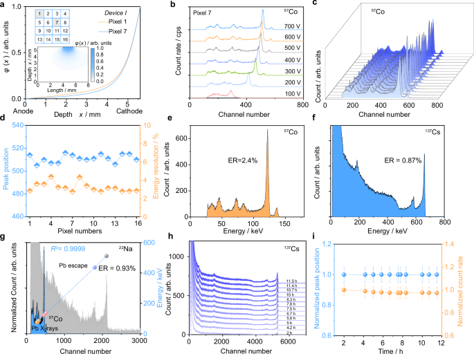
a Weighting potential simulation for pixelated Device I with the pixel size of 1.5 mm and pitch size of 1.6 mm; inset: the positions of 16 pixels and the two-dimensional weighting potential distribution of pixel 7. b 57Co γ-ray spectra of pixelated Device I collected from pixel 7 at different applied voltages with the collection time of 300 s. c The 57Co γ-ray spectra collected from 16 pixelated electrode of Device I under +700 V with the collection time of 300 s. d The ERs and photopeak positions extracted from 16 pixelated energy spectra under +600 V. e The energy spectrum of 57Co γ-ray collected from pixel 14 of Device I. f 137Cs γ-ray spectrum obtained from pixel 14 of Device I under 600 V with the collection time of ~11.5 h. g Linear response of Detector E to different radiation sources. h The stability of spectra of Device I over a period of 11 h under 137Cs γ-source under 600 V. i Variation of peak channel number and count rate (counts per second) over the working time. The error bars represent 5% errors in Gaussian fitting and counting rate uncertainty.
Flood γ-ray imaging was used for the assessment of imaging uniformity with non-collimated γ-ray sources. Fig. 3b depicts the bias-dependent spectra collected from pixelated electrodes when exposed to a non-collimated 57Co γ-ray source. All 16 pixels provided excellent spectroscopic performance with the clearly resolved 122 keV and 136 keV peaks and rich spectral features, including Pb characteristic Kα and Kβ X-rays and their escape peaks (Fig. 3c and Supplementary Fig. 13). The ERs are in the range of 2.7–4.4% and the photopeak positions are within the channel numbers of 505–515, indicating the consistent performance from all pixels (Fig. 3d). The peak-to-valley ratios, which quantify the extent of the tailing on the lower energy side of the full-energy peak, are as high as 7–15 for 16 pixels, superior to that with the ambipolar planar configuration (~3 at 650 V, Supplementary Fig. 11). The champion ER of 2.4% at 122 keV is attained at the bias of 600 V (Fig. 3e). The overall ER is achieved as 2.8% for 122 keV γ-rays by merging all the spectra data after energy calibration (Supplementary Fig. 14), outperforming the previous reported ER of 3.2% in planar configuration30. Meanwhile, Device E also afforded comparable spectroscopic performance with the ER values ranging from 2.8% to 4.9% (Supplementary Fig. 15).
Impressively, Device I yields an unprecedented raw ER of 0.87% at 662 keV under 600 V, exceeding 1.4% of the previously reported 2 × 2 pixelated CsPbBr3 detectors after depth correction30. Note that this ER is, in fact, comparable to the state-of-the-art pixelated CZT detectors and represents an uplift towards the Fano factor-limited ER30. The spectral linearity was determined by various characteristic photopeak energies, with a high correlation coefficient R2 of 0.9999 (Fig. 3g). The 22Na γ-ray spectrum obtained from pixel 16 in Device E shows the outstanding ER of 0.93% at 511 keV. The ERs of other pixels are also consistently superior to 2% for 511 keV γ-rays (Supplementary Fig. 16). The detector performance stability has been confirmed through a continuous measurement with no shifting of the peak position (Fig. 3h). As indicated, over more than 11 h of continuous operation under the bias of 600 V, the channel numbers and the count rate are also unchanged (Fig. 3i).
Fig. 4a shows a pair of typically coincident pulses of a full energy deposition event of a 137Cs γ-ray photon interacting near the anode. 137Cs γ-ray was used here to characterize of response uniformity across the thickness. A digital readout system integrating 17-channel preamplifiers and data acquisition digital cards was developed for sampling and digitizing the output pulse waveforms from 4 × 4 pixelated cathodes, as well as the anode. The non-linear and linear characteristics from pixelated cathode and anode pulses are consistent with the predicted weighting potential distribution (Fig. 4a). Since the inevitable overlapping of the weighting potential distribution or expanding of charge clouds, coincident multiple-pixel responses are anticipated upon a single interaction event due to charge induction or charge sharing among adjacent pixels. This leads to an apparent hump in the low-energy range of the energy spectrum. Note that realizing the capability of 3-D positioning is critical for the proposed ultrahigh-resolution imaging applications, as it minimizes the parallax error in image reconstruction. Accordingly, in order to analyze the depth-of-interaction of various events, we further studied the cathode or anode signal amplitude versus the hole drift time (Fig. 4b). Therefore, by implementing the depth-correction algorithm and removing near-pixel events (25% closest to the cathode) enables further improved ER from 1.9% to 0.91% and the enhanced P/C ratio from 2.0 to 6.6 (Fig. 4c).
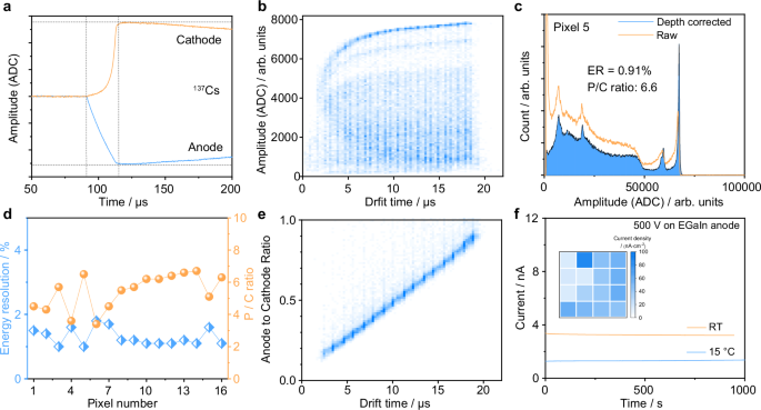
a Measured pulse shape from planar (anode) and pixelated (cathode) electrodes. b Scatter density plot of the γ-ray interaction events collected by a single pixel, rejecting induced signals. c 137Cs γ-ray spectra of pixel 5 by summarizing all events (without any correction, raw data) and after depth correction and removing near-pixel events within 25% of the thickness closest to the cathodes. Over 7 × 10⁶ γ-ray interaction events were recorded in 4 × 4 pixelated detectors over a time period of 10 h. d The ERs and P/C ratios of 16 pixels in Device I after depth correction. e The linear correlation between anode/cathode ratio and drift time. f Leakage current of a pixelated electrode measured at RT and 15 °C; inset: the current density mapping of 16 pixelated electrodes on Device I.
Figure 4d depicts the depth-corrected ER in the range of 0.9–1.6% and P/C ratios of 3.5–6.6 from 16 pixelated electrodes (Fig. 4d and Supplementary Fig. 17), confirming the uniform response across the whole detector volume. Nonetheless, rejecting the near-pixel events certainly lowers the overall efficiency, which in turn requires a more delicate processing algorithm and device optimization for reaching more favorable pixel pitch-to-crystal thickness ratios. As depicted in Fig. 4e, the linear correlation between anode/cathode ratio and drift time indicates a uniform distribution of the electric field. Furthermore, the mobility and lifetime product of hole carrier μτh calculated by the photopeak amplitudes49 is superior to 2.0 × 10⁻² cm2/V (Supplementary Fig. 18).
Note that the low and stable leakage currents are indispensable for maintaining the device with ultra-stable baselines at high voltage, particularly for the pulse digitization process. The overall leakage current for the Device I was demonstrated as ~150 nA under 500 V and gradually decreased to ~55 nA after a period of bias aging (Supplementary Fig. 19a). The guard ring electrode can drain the surface leakage currents, thereby the leakage currents on 16 pixels are reduced to 3.0–5.5 nA (130–240 nA·cm−2) with negligible fluctuation (Supplementary Fig. 19b–d). To further minimize the dark current, active cooling was implemented to maintain the detector temperature at around 15–20 °C to avoid continuous heat dissipation from electronics. Surprisingly, the leakage currents were dramatically reduced to only 0.3–2 nA (15–86 nA·cm−2) on pixelated electrodes (Fig. 4f and Supplementary Fig. 20), ensuring the high electrical stability of the detector.
The long-term stability of CsPbBr3 pixelated detectors has also been examined. Supplementary Fig. 21 illustrates the 57Co γ-ray responses of the freshly prepared CsPbBr3 pixelated Device E and the same detector after 33 days. The detector continued to deliver highly resolved 57Co γ-ray spectra and hardly demonstrated any degradation in detection performance. Specifically, the ERs for 57Co 122 keV γ-rays for 16 pixelated electrodes ranged from 2.7 to 6.5% under 200 V, consistent with the ER of 3.2–5.6% measured from the freshly prepared detector. Additionally, the leakage currents on pixelated electrodes were even lower after 20 days (Supplementary Fig. 22).
Besides the flood γ-ray single-photon imaging, a patterned γ-ray single-photon imaging has also been performed using collimated aqueous solution Na99mTcO4 sources. Primarily, the energy resolving capability for 99mTc 141 keV γ-rays of 16 pixels has been tested initially. As shown in Fig. 5a and Supplementary Fig. 23, all the pixelated electrodes in Device E delivered excellent 99mTc γ-ray spectra, showing well-resolved Pb characteristic X-rays and the escape peaks. The consistent performance from all the pixelated electrodes indicates the prominent response uniformity of Device E, with sharp distribution of ERs in the range of 2–3% and photopeak positions with the channel number of 600–610 (Supplementary Fig. 24a). The champion ER of 2.2% at 141 keV is recorded by pixel 3 (Supplementary Fig. 24b). The overall ER of 2.5% and a high photo-fraction ratio towards 141 keV γ-rays was achieved (Fig. 1b) after energy calibration. Device I also featured impressive distinguishing ability with an overall ER of 3.5% (Supplementary Fig. 25).
a 99mTc γ-ray spectra collected from 16 pixelated electrodes of Device E under +400 V on EGaIn anode with a collection time of 300 s. Diagram of the imaging test for 99mTc point source (b) and line source imaging (c) by pixelated Device E. Note that the data acquisition time was 100-300 s for each pixel. Event counts were acquired using an 8% energy window (135–146 keV) owing to the high ER for every pixelated electrode. d Diagram of the 99mTc column sources with a diameter of 0.7 mm in the Derenzo phantom imaging test. e Image of the single column source at an imaging distance of 2.05 cm.
As a showcase in Fig. 5b, c, 3.5 mm-thick single parallel hole and line collimators made of tungsten were used for 99mTc γ-ray point and line source imaging. The size of the hole diameter and line width are both 0.5 mm (Supplementary Fig. 26). The counting images depicted in Fig. 5b, c for Device E and Supplementary Fig. 27 for Device I distinguish the shapes of the collimators clearly, with only the pixels above the opening displaying expected high counts (Supplementary Figs. 28–31). The intrinsic spatial resolutions for Device E and Device I are 1.2 and 1.6 mm, respectively. The sensitivity is then calculated by integrating all counts in the region of interest (135–146 keV) based on the initial activity of 99mTc γ-ray sources, giving the sensitivities of 0.13% cps/Bq for Device E (point source and line source), 0.059% (point source) and 0.21% (line source) cps/Bq for Device I, respectively (Supplementary Table 5 and Supplementary Note 2). Device I is supposed to possess higher detection sensitivity owing to the larger detector thickness and pixel size. The calculated low sensitivity of 0.059% cps/Bq in the point source imaging of Device I may be attributed to the mismatching of the single-hole collimator and the pixel position, resulting in the counting loss (Supplementary Note 2).
Micro Derenzo phantom imaging has also been performed to evaluate the spatial resolution. Three columnar sources with a diameter of 0.7 mm and depth of 6 mm (Fig. 5d) were placed at a 2.05 cm distance from the detector. The obtained 99mTc γ-ray spectrum features notable scatter events in the low-energy region, but still a high ER of 2.4% (Supplementary Fig. 32). As shown in Fig. 1d, the raw image of three-column sources with a 7 mm interval can be clearly distinguished. The measured spatial resolutions, defined as the full width at the half of maximum (FWHM) of the count profile curves, were 3.2 mm and 3.8 mm (Fig. 1e) for three-column sources along the X direction, which is consistent with the imaging results of a single column source with a less step size (Fig. 5e and Supplementary Fig. 33). It should be emphasized that the detection sensitivity and spatial resolution greatly depends on the imaging distances and collimator design (Supplementary Note 2).
Discussion
In conclusion, we showcase the high-resolution perovskite γ-ray camera for single-photon γ-ray γ-imaging, achieving both high spectral and spatial resolutions. We established the systematic approaches in developing high-performance perovskite pixelated detectors with high uniformity and stability, and in analyzing the multichannel signals for γ-ray single-photon imaging. The non-uniformity of detector performance was discovered through an in-situ PEµM and eliminated by a chemical-mechanical processing approach for near-unity CCE. The state-of-the-art resolving capability, 2.2% at 99mTc 141 keV, 2.4% at 57Co 122 keV, 0.93% at 22Na 511 keV, and 0.87% at 137Cs 662 keV γ-rays, is achieved by a pixelated CsPbBr3 detector. 99mTc point and line source imaging shows a high sensitivity of 0.13%–0.21% cps/Bq and intrinsic spatial resolution of 1.2 and 1.6 mm. The spatial resolution (FWHM) as measured using the Derenzo phantom is about 3.2–3.8 mm. Our findings attest to the suitability of the perovskite semiconductor as a practical, low-cost technology for nuclear medicine γ-ray imaging. Therefore, it is anticipated that the realization and exemplification of the protocols of high-resolution perovskite semiconductor for γ-ray imaging shall spark great interest for metabolic functional imaging in nuclear medicine applications.
Methods
Crystal growth
The improved Bridgman method was employed for the growth of high-quality and large-volume CsPbBr3 single crystals29. Silica tubes with an inner diameter of 30 mm were preprocessed to form a conical-shaped end. The precursors of CsBr and PbBr2 in a 1:1 stoichiometric ratio were sealed in the silica tube. The solid-state reaction for CsPbBr3 synthesis in the sealed tube was carried out at 580 °C. Both the synthesis and subsequent growth processes were performed under vacuum conditions with a residual pressure of 5 × 10⁻⁴ Pa. Notably, a custom-designed four-zone vertical Bridgman furnace was used to achieve a precisely regulated temperature field, thereby avoiding thermally induced cracking and supercooling. During the crystal growth process, the sealed tube was heated up to 600 °C in 10 h and then maintained at this temperature for 12 h. The crystal ingot gradually descended through the furnace at a rate of 1.0 mm per hour. After growth, the ingot was cooled to 200 °C and subsequently cooled to room temperature at a cooling rate of 5 K per hour.
Sample processing
The grown ingot was sliced into circular wafers and then into desired shapes using a wire saw equipped with a diamond wire with a diameter of 0.3 mm. A slower cutting speed of 0.5–1 mm·s−1 was preferred to avoid forming deep cutting impressions into the wafers. Subsequently, mechanical polishing was performed sequentially using SiC grinding paper. The polished surfaces were carefully cleaned with toluene and then etched by dipping into a mixture of DMSO solvent and lubricant (added for diluting DMSO) for 30 s to eliminate the scratches or scuffs. After etching, the wafers were rinsed in toluene again to remove the residual DMSO and other contaminants before electrode deposition.
General properties characterization for single-crystal wafers
The photoluminescence (PL) spectra and lifetimes were recorded on an Edinburgh Instruments FS5 spectrofluorometer at RT using a 375 or 405 nm pulsed laser diode as the excitation source. The surface roughness was measured using a Bruker Dimension ICON atomic force microscope. The contour arithmetic mean deviation Ra has been utilized for the surface roughness assessment. The equation is defined as \({R}_{a}\,=\,\frac{1}{N}{\sum}_{j=1}^{N}|{z}_{j}|\), in which \({z}_{j}\) refers to the height deviations taken from any point on the surface to the mean data plane.
Fabrication of planar-type and pixelated detectors
Four kinds of metal electrodes with low work function were selected to fabricate Schottky-type planar detectors with Au: Au/CsPbBr3/Bi, Au/CsPbBr3/In, Au/CsPbBr3/Cr, and Au/CsPbBr3/EInGa. The full planar Bi and Cr contacts were thermally evaporated on the surfaces with a thickness of 70–100 nm. Plasma-enhanced magnetron sputtering method was performed for the deposition of 70 nm of In contact on the wafers. The Au electrode was prepared by brushing Au paint or thermal evaporation (70–100 nm). The EGaIn contact was formed by spreading GaIn eutectic liquid on the surface of the CsPbBr3 wafer. All the electrodes were connected to Cu wires using Ag paint and then to the outer readout circuits.
Au and EGaIn contact combinations were selected for the fabrication of CsPbBr3 4 × 4 pixelated detectors. The full planar EGaIn contact was prepared as mentioned above. The pixelated Au electrode patterns with a thickness of 100 nm were deposited through the thermal evaporation method using photomasks with different pixel and pitch sizes. For Device E, the pixel and pitch sizes are 1.0 × 1.0 mm2 and 1.2 mm; for Device I, the sizes are 1.5 × 1.5 mm2 and 1.6 mm. 16 pixelated Au electrodes and a guard ring were wire-connected to the nuclear electronic readout system using Ag paint. Both planar and pixelated detectors were encapsulated by paraffin wax, as reported before.
Photoelectrical response micromapping (PEµM) measurement
In order to evaluate the impact of scratches on the charge collection, a micro-scale transient pulse height mapping measurement (Supplementary Fig. 6) was performed on an Au/CsPbBr3/Bi device. One CsPbBr3 crystal was fabricated into the detector two times to eliminate crystal-to-crystal quality variation, but with different surface treatments. The first time the device was fabricated, the crystal surface was only mechanically polished, generating numerous scratches. During the second fabrication, the surface previously mechanically polished was significantly reduced in scratches by employing dimethyl sulfoxide (DMSO) for etching. A pulsed laser of 482 nm with a duration of 75 ps and a 2 kHz repetition rate was used as the excitation source, which is analogous to a γ-ray source for the generation of electrons and holes in the detector. The laser beam is focused on the tested device with a 20x microscope objective, resulting in a spot approximately 8 μm in diameter. A negative bias voltage was applied to the bottom Au contact, and the laser was irradiated from the Bi contact. An eV-550 preamplifier was connected to detectors for the initial signal amplification, outputting voltage pulses. Subsequently, the transient pulses were further amplified and shaped using the ORTEC model 572 A amplifier, forming Gaussian-shaped pulses recorded by an oscilloscope. The device was mounted on a motorized X–Y scanning stage, translating the sample to the region of interest for pulse acquisition at a determined step of 1 μm. Both the position information and the pulse height could be extracted in a one-to-one correspondence, generating transient pulse height mapping. Since the interaction occurred near the surface, the induced signals are mainly caused by the drift of holes, and the impact of surface scratches on charge collection can be reflected by the pulse height values at that specific position.
The trap density (ntrap) for CsPbBr3 crystals treated by only mechanical polishing and a combination of mechanical polishing and DMSO etching was assessed using SCLC measurement with a typical structure of Au/CsPbBr3/Au50.
Electrical properties and detector performance assessment
The J–V characterizations of detectors were measured on a Keithley 6517B electrometer under dark conditions. A diffusion model has been proposed for modeling the electrical properties of metal-CsPbBr3 Schottky junctions (Supplementary Fig. 9b). The current density J under the reverse bias V can be described as:
$$J=\,\frac{{q}^{2}\mu {N}_{c}{N}_{i}}{\varepsilon }\,\left[\frac{\varepsilon }{q{N}_{i}d}\,\left(V+{V}_{{in}}\right)\,+\,\frac{d}{2}\right]\left(1-{e}^{-\frac{{qv}}{{kT}}}\right){e}^{-\frac{q\varphi }{{kT}}}$$
(1)
where q is the electron charge, μ is the carrier mobility (the hole mobility of CsPbBr3 is set as 31 cm2·V·s−1 according to the 241Am 5.5 MeV α particles response measurement), Nc is the effective density of states in the conduction band, Ni is the concentration of the ionized donor/acceptor centers, ε is the electrical permittivity in the crystal (for CsPbBr3, the relative dielectric constant is about 19.251), d is the thickness of the device, Vin is built-in internal electric field (zero-bias potential, Vin is less than 1 V here), k is Boltzmann’s constant, T is temperature, φ is the Schottky barrier. Specifically, Nc is determined as 2(2πm*kT/h2)3/2, where m* is the effective mass of the carrier and h is the Planck constant.
γ-ray detection measurements
Various γ-ray and α particle sources, including 1 μCi 241Am, 14 μCi 57Co, 99mTc, 20 μCi 22Na, and 40 kBq 137Cs, were used in this work to evaluate the detector performance. For planar detectors, which afford only one readout channel, an eV-550 preamplifier was connected to detectors placed in a shielding box with the Au electrode face down. The negative bias voltage was applied to the bottom Au contact, and the γ-rays or α particles were incident from the top electrode. The induced signals from the detector were amplified initially by a preamplifier, outputting voltage pulses with an amplitude of a few to tens mV. Subsequently, the transient pulses were further amplified and shaped using an ORTEC model 572A amplifier with a shaping time of 0.5–10 μs. The signals from the main amplifier with amplitudes from several hundreds of mV to a few V were then analyzed by a dual 16 K input multichannel analyzer (model ASPEC-927) and analog-to-digital converter, finally generating a response spectrum displayed on MAESTRO-32 software.
The mobility was estimated based on the average rise times of transient pulses, according to the equation \(\mu \,={d}^{2}/\left({t}_{r}V\right)\), in which d is the thickness of the detector (Supplementary Fig. 4). The mobility-lifetime product μτ could be directly calculated by measuring the photopeak amplitudes of events originating near the anode surface at bias voltages V1 and V2 according to the following equation:
$${\mu \tau }_{h}\,=\,\frac{{D}^{2}}{{{\mathrm{ln}}}(\frac{N1}{N2})}\,\left(\frac{1}{{V}_{2}}-\frac{1}{{V}_{1}}\right)$$
(2)
where D is the detector thickness; N1 and N2 are the photopeak amplitudes of the events near the anode under the bias voltage of V1 and V2, respectively (Supplementary Fig. 18).
Detection measurements on 4 × 4 pixelated detectors
For pixelated detectors, a positive bias voltage was applied to the bottom EGaIn electrode, and all the pixelated and guard-ring Au contacts were grounded. During the γ-ray response measurements, the 241Am, 57Co, 99mTc γ-ray sources were placed under the detector, while the 22Na, 137Cs γ-ray sources were located on the top. The collection of response spectra from the 16 pixelated Au electrodes and planar EGaIn contact was similar to that of a planar detector. An integrated 17-channel preamplifiers were designed to process the induced signals from both pixelated and planar electrodes simultaneously. Using two model 572A amplifiers and a dual 16 K input multichannel analyzer, the energy spectra of two channels could be collected simultaneously. The gain was set to be 0.8 × 100, and the shaping time was 10 μs. Energy calibration of the nuclear electronics system and gain normalization of the 17 preamplifiers were performed using a pulse generator.
Additionally, a digital readout system containing three 8-channel data acquisition cards was used for the capture of output waveforms from 17 preamplifiers and shaped signals of planar EGaIn electrode, which has been set to trigger (Supplementary Fig. 34). To eliminate the noise interference on the determination of amplitude and rise time, a mean filter has been performed on the preamplifier waveforms. The difference in event interaction time from the raw planar waveform and the end of the charge collection time from the raw pixel waveform was defined as the hole drift time, and event interaction depth was indicated under the assumption of a uniform electric field in the detector. The values of t1 and t2 were extracted by using a constant fraction scheme. Waveform processing was performed by using a digital CR-(RC)4 shaper with an RC constant of 5. The range of drift times was divided into 30 depth bins, and the photopeak centroids in each bin were aligned to the maximum centroid across all depths and all pixels, yielding a depth-gain correction curve. To apply the correction, the depth of interaction of each event is calculated based on the drift time. Assuming a good linearity of response, aligning peak centroids also aligns other spectral features, such as the Compton edge and backscatter peak, as well as correcting for the gain variations between different readout channels.
γ-ray imaging test of pixelated detectors
An aqueous solution of Na99mTcO4 was sealed in quartz capillary tubes with an inner diameter of 0.5 mm and an external diameter of 1.0 mm (Supplementary Fig. 26a) in the γ-ray imaging test. Single parallel hole and line collimators made of tungsten with a thickness of 4.5 mm were separately applied in the point and linear source imaging of 99mTc. The configurations and sizes of the collimators are detailed in Supplementary Fig. 26b–g. The single parallel hole collimator features a hole with a 0.5 mm inner diameter; the line collimator measures 0.5 mm in width and 6.0 mm in length. A slot with a depth of 1.0 mm was carved into the underside for the placement of capillary tubes; thus, the depth of both collimators is 3.5 mm. The collimators and the 99mTc γ-ray sources were positioned beneath the detector. The acquisition of energy spectra from 16 pixelated electrodes was accomplished using integrated 17-channel preamplifiers and an ORTEC nuclear electronic system. The resulting image was generated by plotting the position of 16 pixels against the corresponding counts within an energy window of 8% centered at 141 keV (135–146 keV).
For micro Derenzo phantom imaging, Na99mTcO4 aqueous solution was injected into one or three columns with a diameter of 0.7 mm. The single parallel hole collimator was used to achieve single pixel readout. The micro Derenzo phantom was placed on a two-dimensional motion control platform and progressively moved in increments of 0.3 or 0.4 mm along the horizontal X–Y direction. Energy spectra were collected at fixed positions for 30 s after each step movement. Similarly, the image was derived by plotting the position against the corresponding counts in the energy window of 20%.
Data availability
The data that support the plots within this paper and other findings of this study are available from the corresponding author upon request.
References
Cherry, S. R., Sorenson, J. A. & Phelps, M. E. Physics in Nuclear Medicine (Elsevier, 2012).
Boros, E. & Packard, A. B. Radioactive transition metals for imaging and therapy. Chem. Rev. 119, 870–901 (2018).
James, M. L. & Gambhir, S. S. A molecular imaging primer: modalities, imaging agents, and applications. Physiol. Rev. 92, 897–965 (2012).
Weissleder, R. Scaling down imaging: molecular mapping of cancer in mice. Nat. Rev. Cancer 2, 11–18 (2002).
Mariani, G. et al. A review on the clinical uses of SPECT/CT. Eur. J. Nucl. Med. Mol. Imaging 37, 1959–1985 (2010).
Ljungberg, M. & Pretorius, P. H. SPECT/CT: an update on technological developments and clinical applications. Brit. J. Radiol. 91, 20160402 (2018).
Enlow, E. & Abbaszadeh, S. State-of-the-art challenges and emerging technologies in radiation detection for nuclear medicine imaging: a review. Front. Phys. 11, 1106546 (2023).
Anger, H. O. Scintillation camera. Rev. Sci. Instrum. 29, 27–33 (1958).
Dorbala, S. et al. Single photon emission computed tomography (SPECT) myocardial perfusion imaging guidelines: instrumentation, acquisition, processing, and interpretation. J. Nucl. Cardiol. 25, 1784–1846 (2018).
Cates, J. W., Gu, Y. & Levin, C. S. Direct conversion semiconductor detectors in positron emission tomography. Mod. Phys. Lett. A 30, 1530011 (2015).
Wu, D. et al. Comparison of CZT SPECT and conventional SPECT for assessment of contractile function, mechanical synchrony and myocardial scar in patients with heart failure. J. Nucl. Cardiol. 26, 443–452 (2017).
Johnson, R. D. et al. Introduction to the D-SPECT for technologists: workflow using a dedicated digital cardiac camera. J. Nucl. Med. Technol. 48, 297–303 (2020).
Ritt, P. Recent Developments in SPECT/CT. Semin. Nucl. Med. 52, 276–285 (2022).
Niimi, T., Nanasato, M., Sugimoto, M. & Maeda, H. Evaluation of cadmium-zinc-telluride detector-based single-photon emission computed tomography for nuclear cardiology: a comparison with conventional Anger single-photon emission computed tomography. Nucl. Med. Mol. Imaging 51, 331–337 (2017).
He, Y., Hadar, I. & Kanatzidis, M. G. Detecting ionizing radiation using halide perovskite semiconductors processed through solution and alternative methods. Nat. Photonics 16, 14–26 (2022).
Deumel, S. et al. High-sensitivity high-resolution X-ray imaging with soft-sintered metal halide perovskites. Nat. Electron. 4, 681–688 (2021).
He, Y. et al. Sensitivity and detection limit of spectroscopic‐grade perovskite CsPbBr3 crystal for hard X‐Ray detection. Adv. Funct. Mater. 32, 2112925 (2022).
Kim, Y. C. et al. Printable organometallic perovskite enables large-area, low-dose X-ray imaging. Nature 550, 87–91 (2017).
He, Y. et al. Demonstration of energy-resolved gamma-ray detection at room temperature by the CsPbCl3 perovskite semiconductor. J. Am. Chem. Soc. 143, 2068–2077 (2021).
He, Y. et al. Resolving the energy of gamma-ray photons with MAPbI3 single crystals. ACS Photonics 5, 4132–4138 (2018).
Kakavelakis, G. et al. Metal halide perovskites for high-energy radiation detection. Adv. Sci. 7, 2002098 (2020).
Yakunin, S. et al. Detection of gamma photons using solution-grown single crystals of hybrid lead halide perovskites. Nat. Photonics 10, 585–589 (2016).
Huang, J. et al. High yield solution growth of FACsPbBr3 single crystals with low defect density for gamma-ray spectroscopy. Nat. Photonics 17, 315–323 (2023).
Zhao, L. et al. High-yield growth of FACsPbBr3 single crystals with low defect density from mixed solvents for gamma-ray spectroscopy. Nat. Photonics 17, 315–323 (2023).
Qin, H. et al. Virtual frisch grid perovskite CsPbBr3 semiconductor with 2.2-centimeter thickness for high energy resolution gamma-ray spectrometer. Nat. Commun. 16, 158 (2025).
Shen, N. et al. Enhancing gamma-ray spectral resolution in perovskite CsPbBr3 detectors through dark current reduction with guard ring electrodes. ACS Photonics 11, 3662–3671 (2024).
Xiao, B. et al. Ambipolar charge transport in perovskite CsPbBr3 gamma-ray detectors with superior uniformity and spectral resolution by zone refining processing. Adv. Sci. 12, e2501875 (2025).
Stoumpos, C. C. et al. Crystal growth of the perovskite semiconductor CsPbBr3: a new material for high-energy radiation detection. Cryst. Growth Des. 13, 2722–2727 (2013).
He, Y. et al. High spectral resolution of gamma-rays at room temperature by perovskite CsPbBr3 single crystals. Nat. Commun. 9, 1609 (2018).
He, Y. et al. CsPbBr3 perovskite detectors with 1.4% energy resolution for high-energy γ-rays. Nat. Photonics 15, 36–42 (2021).
Zhao, L. et al. Surface-defect-passivation-enabled near-unity charge collection efficiency in bromide-based perovskite gamma-ray spectrum devices. Nat. Photonics 18, 250 (2024).
Knoll, G. F. Radiation Detection and Measurement (Wiley, 2010).
McGregor, D. S. & Hermon, H. Room-temperature compound semiconductor radiation detectors. Nucl. Instrum. Meth. Phys. Res. A 395, 101–124 (1997).
Harrison, M. J., McGregor, D. S. & Doty, F. P. Fano factor and nonuniformities affecting charge transport in semiconductors. Phys. Rev. B 77, 195207 (2008).
Zhou, Y. et al. Self-powered perovskite photon-counting detectors. Nature 616, 712–718 (2023).
Chung, D. Y. et al. Growth of high-purity CsPbBr3 crystals for enhanced gamma-ray detection. Cryst. Growth Des. 24, 9590–9600 (2024).
Gul, R. et al. Point defects in CdZnTe crystals grown by different techniques. J. Electron. Mater. 40, 274–279 (2011).
Aqariden, F. et al. Influence of surface polishing on the structural and electronic properties of CdZnTe surfaces. J. Electron. Mater. 41, 2893–2898 (2012).
Tari, S. et al. Structural and electronic properties of gold contacts on CdZnTe with different surface finishes for radiation detector applications. J. Electron. Mater. 43, 2978–2983 (2014).
Gao, F., Zhao, Y., Zhang, X. & You, J. Recent progresses on defect passivation toward efficient perovskite solar cells. Adv. Energy Mater. 10, 1902650 (2020).
Yang, S. et al. Stabilizing halide perovskite surfaces for solar cell operation with wide-bandgap lead oxysalts. Science 365, 473–478 (2019).
Tan, S. et al. Stability-limiting heterointerfaces of perovskite photovoltaics. Nature 605, 268–273 (2022).
Min, H. et al. Perovskite solar cells with atomically coherent interlayers on SnO2 electrodes. Nature 598, 444–450 (2021).
Nayak, P. K. et al. Mechanism for rapid growth of organic-inorganic halide perovskite crystals. Nat. Commun. 7, 13303 (2016).
Bai, R. et al. Kinetic modulation-eliminated precursor liquid inclusions in solution-grown CsPbBr3 bulk crystals for gamma-ray detection. J. Mater. Chem. A 12, 13925–13932 (2024).
He, Z. Review of the Shockley–Ramo theorem and its application in semiconductor gamma-ray detectors. Nucl. Instrum. Methods Phys. Res. A 463, 250–267 (2001).
Shockley, W. Currents to conductors induced by a moving point charge. J. Appl. Phys. 9, 635–636 (1938).
He, Y. et al. Perovskite CsPbBr3 single crystal detector for alpha-particle spectroscopy. Nucl. Instrum. Methods Phys. Res. A 922, 217–221 (2019).
He, Z., Knoll, G. F. & Wehe, D. K. Direct measurement of product of the electron mobility and mean free drift time of CdZnTe semiconductors using position sensitive single polarity charge sensing detectors. J. Appl. Phys. 84, 5566–5569 (1998).
Dong, Q. et al. Electron-hole diffusion lengths 175 μm in solution-grown CH3NH3PbI3 single crystals. Science 347, 967–970 (2015).
Schlaus, A. P. et al. How lasing happens in CsPbBr3 perovskite nanowires. Nat. Commun. 10, 265 (2019).
Wagenaar, D. J. CdTe and CdZnTe semiconductor detectors for nuclear medicine imaging. in Emission Tomography (eds Wernick, M. N. & Aarsvold, J. N.) 269–291 (Elsevier Academic Press, 2004).
Acknowledgements
This work was supported by the National Key R&D Program of China (2021YFF0502600) and the National Natural Science Foundation of China (U2267211) to Y.H., Jiangsu Natural Science Foundation (BK20240822) to Q.S. At Northwestern University, the work is supported by the Defense Threat Reduction Agency under Award No. HDTRA12020002 to the Consortium for Interaction of Ionizing Radiation with Matter—University Research Alliance (IIRM-URA) to M.G.K. Any opinions, findings, conclusions, or recommendations expressed in this material are those of the authors and do not necessarily reflect the views of the Defense Threat Reduction Agency.
Ethics declarations
Competing interests
The authors declare no competing interests.
Peer review
Peer review information
Nature Communications thanks the anonymous reviewer(s) for their contribution to the peer review of this work. A peer review file is available.
Additional information
Publisher’s note Springer Nature remains neutral with regard to jurisdictional claims in published maps and institutional affiliations.
Supplementary information
Rights and permissions
Open Access This article is licensed under a Creative Commons Attribution-NonCommercial-NoDerivatives 4.0 International License, which permits any non-commercial use, sharing, distribution and reproduction in any medium or format, as long as you give appropriate credit to the original author(s) and the source, provide a link to the Creative Commons licence, and indicate if you modified the licensed material. You do not have permission under this licence to share adapted material derived from this article or parts of it. The images or other third party material in this article are included in the article’s Creative Commons licence, unless indicated otherwise in a credit line to the material. If material is not included in the article’s Creative Commons licence and your intended use is not permitted by statutory regulation or exceeds the permitted use, you will need to obtain permission directly from the copyright holder. To view a copy of this licence, visit http://creativecommons.org/licenses/by-nc-nd/4.0/.
About this article
Cite this article
Shen, N., He, X., Gao, T. et al. Single photon γ-ray imaging with high energy and spatial resolution perovskite semiconductor for nuclear medicine. Nat Commun 16, 8113 (2025). https://doi.org/10.1038/s41467-025-63400-7
Received: 01 January 2025
Accepted: 12 August 2025
Published: 30 August 2025
DOI: https://doi.org/10.1038/s41467-025-63400-7